Intel Architecture Day 21: Alder Lake, Arc, Sapphire Rapids And More Revealed
Under The Hood Of Alder Lake – Intel’s Hybrid Competitor For Desktop And Mobile
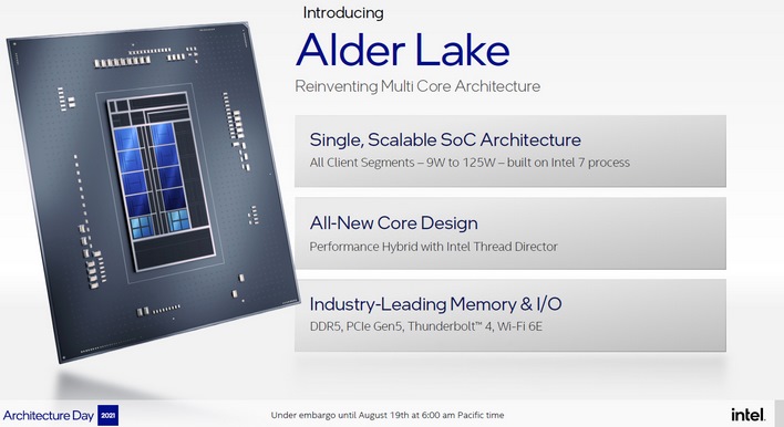
Intel actually backed into its Alder Lake deep dive, covering its core architecture rather than product instantiations first, but we felt it might be more logical to look at the high level chip derivatives first and then go under the hood for a look at cores, caches and plumbing. First and foremost, Alder Lake is intended to be a single, scalable system-on-chip (SoC) CPU architecture that is designed to address PC client platforms from ultra-mobile solutions at 9 Watts to high performance 125 Watt+ desktop solutions and everything in between.Alder Lake is built on the Intel 7 process node, previously known as 10nm Enhanced SuperFin. As we’ve previously reported, it is a hybrid big.Little design approach, with both Efficiency core and larger Performance core elements, along with a new innovation called Thread Director which we’ll get to shortly.
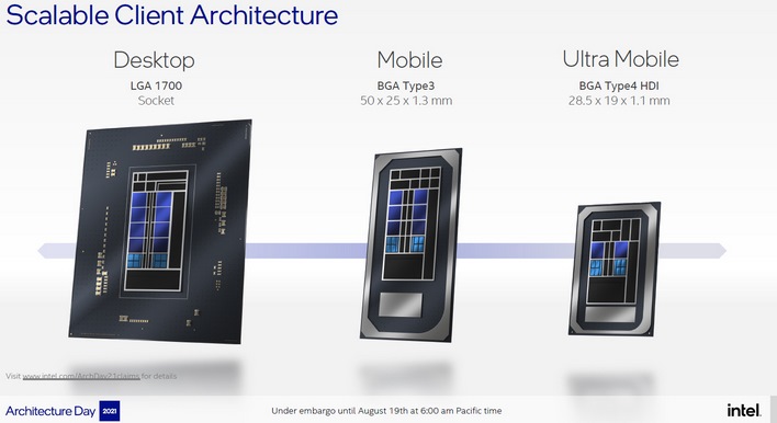
Also on board is a bevy of the latest memory and IO connectivity options including DDR5 memory support, PCI Express Gen 5, Thunderbolt 4 and WiFi-6E connectivity. As you can see here, Intel will build up Alder Lake into various platform implementations, pulling building blocks together, like Performance Cores (P-Core), Efficiency Cores (E-Core), TBT (Thunderbolt), IPU (Image Processing Unit for cameras), ect., along with graphics Execution Units (EU), depending on specific platform requirements. Note that the graphics EUs in Alder Lake are actually of Xe-LP vintage (even on desktop) and not Intel’s new discrete desktop Arc GPU cores. Also note that desktop Alder Lake will only have up to 32 EUs on board, versus up to 96 on mobile platforms.
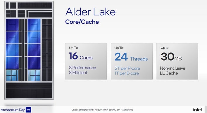
All told, Alder Lake will scale up to 16-core, 24-thread versions, with P-Cores supporting HyperThreading and each E-Core supporting a single thread. Currently, Intel is showing an 8+8 max configuration. So if you do the math, that’s 8 P-Cores supporting 16 threads and 8 E-Cores supporting another 8 threads for a total of 24. Also on board is up to 30MB of Last Level Cache (L3), as well as a memory controller that supports up to DDR5-4800 MHz speeds, LP5-5200, DDR4-3200 and LP4x-4266, all with overclocking support as well.
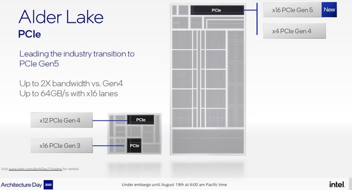
In terms of serial connectivity, Alder Lake desktop versions will offer16 lanes of PCIe Gen 5 and 4 lanes of PCIe Gen 4 connectivity right off the root CPU complex and another 28 lanes of PCIe 4 and PCIe 3 off the PCH (Platform Controller Hub). Of note, that X16 Gen 5 link will support a shiny new next-gen GPU nicely, while that X4 PCI4 Gen 4 link will support a speedy PCIe Gen 4 SSD, both hanging right off the CPU.
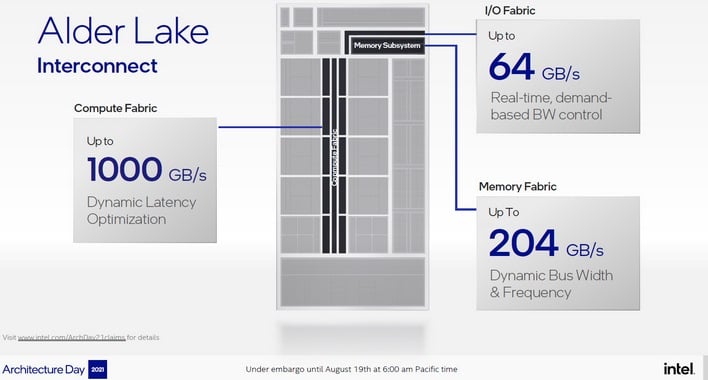
And finally, plumbing all those cores, caches and IO together is no less than three high speed interconnect fabrics, for IO, memory and compute. Each of the fabrics are optimized for either latency, bandwidth or bus width and speed, depending on the functional block requirement. For example, the CPU block’s Compute Fabric supports up to 1000 GB/s of bandwidth with dynamic latency optimization, while the Memory Fabric has flexibility for the various bus widths and clock speeds of the different DDR DRAM memory technologies it needs to support. And so, with the high-level stuff laid out, let’s drop down a peg to some of the intimate details of Alder Lake’s Efficiency and Performance cores.
Alder Lake Efficient-core, Performance-core And Thread Director
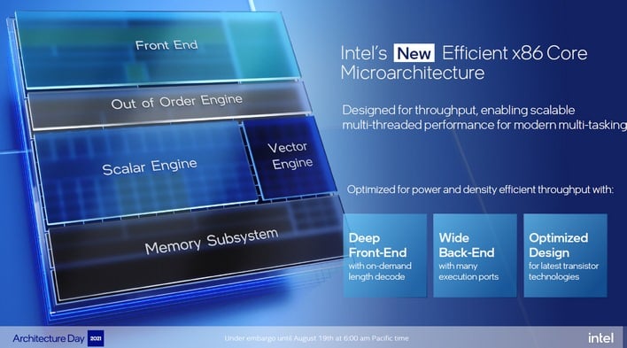
Previously known under the code name Gracemont, Intel claims Alder Lake's new Efficient-core architecture is the most efficient X86 microarchitecture the company has ever delivered. It is highly optimized for silicon area too, such that roughly four Efficient-cores can fit into the die real estate of just one previous-gen Skylake CPU core, while offering improved performance, power efficiency or both. Efficient-core is also designed to run at lower voltages and power envelopes, but with the ability to scale up to higher clock speeds for heavier workloads when necessary.
As, we noted earlier, Intel's Efficient-core architecture does not support HyperThreading (simultaneous multithreading) though there are a number of advancements in the evolution of the Gracemont core architecture that allow it to scale performance dramatically and at lower power than previous-gen Intel architectures. Some of the major enhancements to Efficient-core that improve its IPC (Instructions Per clock Cycle) throughput are the following:
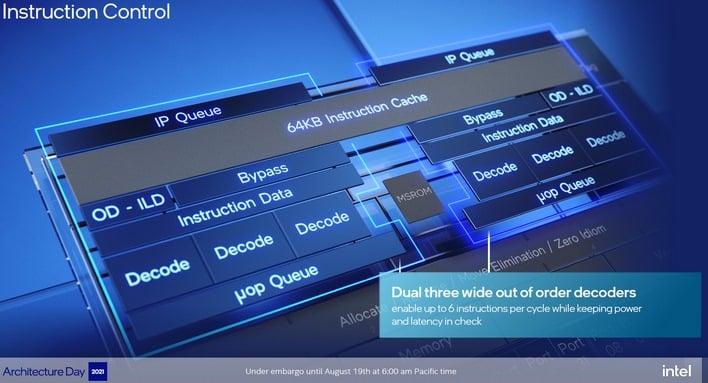
- Larger branch cache and 64KB instruction cache to improve branch prediction and throughput without having to go off-chip into main memory.
- New and improved out-of-order decoders that enable up to six instructions per cycle
- A wider data execution back-end for better discovery and execution of data parallelism
- Robust security control-flow and virtualization protection
- AVX ISA and new instructions for integer AI throughput with Intel DL-Boost Vector Neural Network Instructions
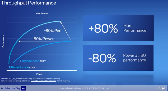
That larger instruction cache is twice the size of Intel's Skylake architecture and it can really help mitigate latency and improve bandwidth as instructions are fed to the core. Intel is comparing its Gracemont Efficient-core architecture to Skylake and relatively, the company claims Efficient-core achieves 40% better performance at the same power envelope or can deliver the same performance at a 40% power reduction.
At scale, a cluster of 4 Efficient-cores will deliver 80% better performance than two Skylake cores (4 threads with HT), or offer the same performance with an 80% power reduction. Couple that with the silicon real estate savings we talked about earlier, where those 4 Efficient-cores fit in the same silicon area of just one Skylake core, and Intel has what sounds like a proverbial win-win on its hands, with a major single-thread performance lift and massive silicon area savings per core implementation. That said, let’s look at the bigger iron Intel Performance-core architecture a bit closer as well, to see what it has in store.
Intel Golden Cove Is Go As Performance-core
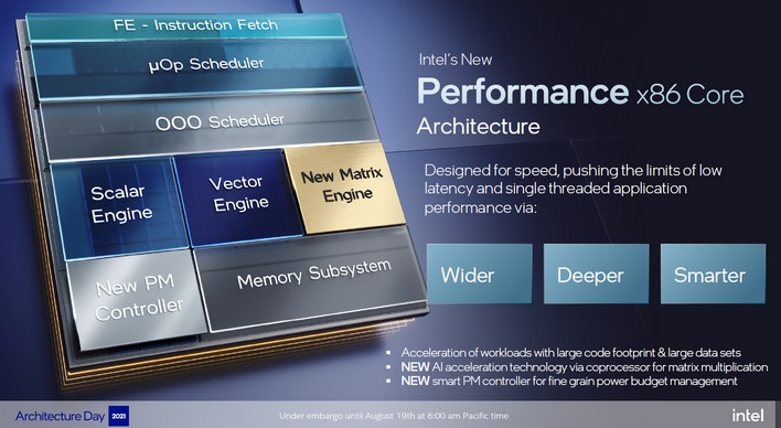
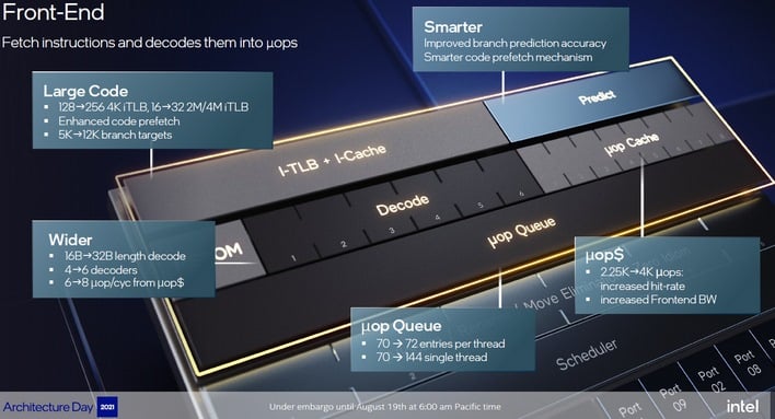
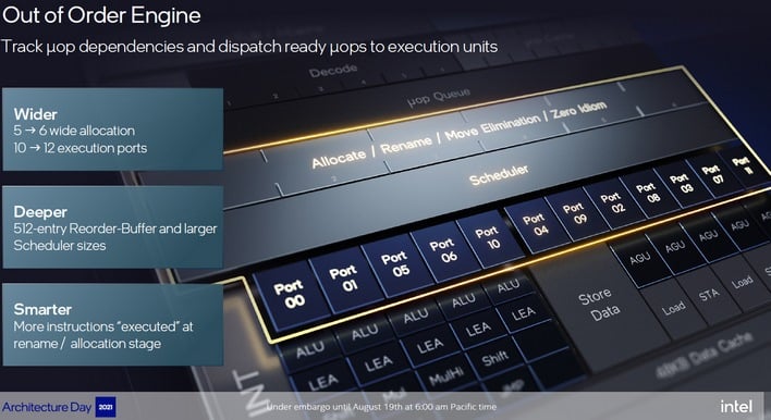
Intel’s new Performance-core architecture known by the code name Golden Cove, is designed for low latency, flat out single-threaded throughput, and better support for larger more complex and diverse applications. It has a larger, more robust front-end for instruction fetch and decode, as well as a “wider, deeper and smarter” out-of-order processing engine with improved branch prediction accuracy, as well as reduced L1 cache latencies and L2 cache bandwidth optimization.
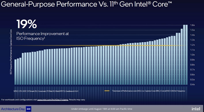
All told Intel, is making the following claims about its Performance-core architecture versus the previous gen Cypress Cove at ISO frequency (like clock speeds)…
- A 19% average performance lift over a wide range of general purpose workloads versus Intel’s current 11th Gen Core processors
- Better memory parallelism and improved execution parallelism with lower latency and support for bigger application footprints.
- Support for Intel Advanced Matrix Extensions (AMX) for data center products based on Alder Lake architecture that includes hardware-assisted processing for faster matrix multiply operations in AI acceleration.
As you can see in the graph above, Intel is illustrating the geometric mean performance gain of Alder Lake's Performance-core versus its current 11th Gen Core architecture code named Cypress Cove. The benchmark metrics here (if you scan the fine print foot notes) are a mix of tests, including SPEC CPU 2017, SYSmark 25, Crossmark, PCMark 10, WebXPRT3, and Geekbench 5.4.1. As you can see, on average there's about a 19% lift, while some results are 1.6X (60%) though a couple actually do land right around the 1X performance line.
Also, It’s important to note that Alder Lake’s Performance-core AMX hardware engine is targeted for data center (Sapphire Rapids Xeon) products only for now and will not be in Alder Lake consumer or enterprise client processor implementations. However, Intel Advanced Matrix Extensions and the Tiled Matrix Multiplication Accelerator in Xeon versions of Alder Lake are claimed to offer an 8X uplift in int8 precision throughput, which will be a key differentiator in AI inferencing applications.
For So Many Threads And Core Types, Intel Designed The Thread Director
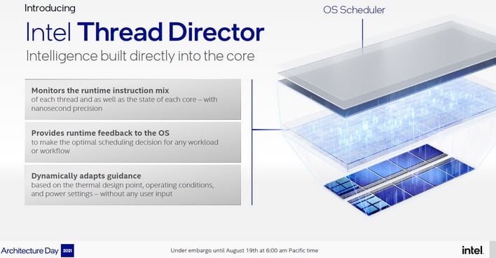
Intel’s Thread Director unveiling was a key disclosure that gave us a bit of an ah-ha moment, with respect to our recent findings on why Windows 11 seems to show a slight performance lift for Intel’s ultra-low power Lakefield hybrid processor architecture. We're told Lakefield has a similar hardware thread management resource on board, but it’s also clear Intel and Microsoft have been working closely on hybrid CPU microarchitecture optimizations for some time. Regardless, Intel Thread Director in Alder Lake is a hardware level thread analyzer and scheduler that, as Intel explains “provides runtime feedback” to the OS for optimal scheduling decisions with any workload. It also dynamically adapts to thermals, load and power requirements on the fly without any user input. In fact, Thread Director will work in conjunction with Windows 11 and is intended to be transparent to the user. In short, you won’t have a switch for it. It’s just always on, doing its thing, all the time.
Here’s a rather useful demo video from Intel that shows you specifically how Thread Director, traffic cop that it is, handles workloads…
One aspect of Thread Director that’s unclear – though we tried hard to tack Intel down on this – is that the technology seems to require Windows 11 for fully optimized support. Though Windows 10 has thread-level awareness of hybrid big.Little architectures, as evidenced by Redmond’s embracing of Snapdragon PCs and the like, the Intel representatives we asked were non-committal on whether Alder Lake would perform the same on Windows 11 as it would on Windows 10. Our hunch is that Windows 11 will be required for the full Alder Lake performance experience, at least in the early stages. How much of a performance delta there is currently is anyone’s guess, and the open source community, with respect to Linux, will obviously need to adopt Intel’s new hardware resources for Thread Director as well.
Intel Sneak Peeks Arc Discrete Graphics For Gamers, And It Looks Good
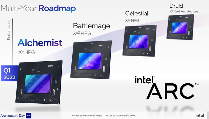
Intel’s Xe-HPG (High Performance Gaming) discrete graphics architecture was teased to us just last week. It is designed to scale from laptops to high-performance gaming and content creation desktops. The company revealed that its Alchemist family of GPUs that are coming to market in Q1 2022 will retail under the Intel Arc brand of graphic cards, and leverage a highly scalable Intel Xe-HPG microarchitecture.In fact, Intel’s roadmap consists of Alchemist GPU core products, and follow-on Battlemage, Celestial and Druid GPU-based products. Notice the simple A-B-C progression here with game character-centric motif. Kudos Intel, simple is good and so is relating to some of the classic game character types as well. The company showcased its Alchemist-based Arc graphics products in live gameplay in several top tier game engines, like Unreal Engine 5, Crysis Remastered, Metro Exodus, and Forza Horizon 4. These demos also showcased leading-edge DirectX 12 Ultimate rendering technologies like Mesh Shaders, Variable Rate Shading, Real-Time Ray Tracing and something called XeSS or Intel Xe Super Sampling, which we’ll circle back on shortly. However, key take-aways from Intel’s Arc unveil were the following:
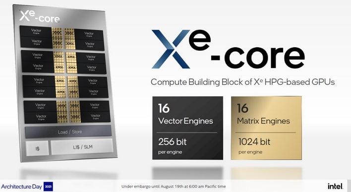
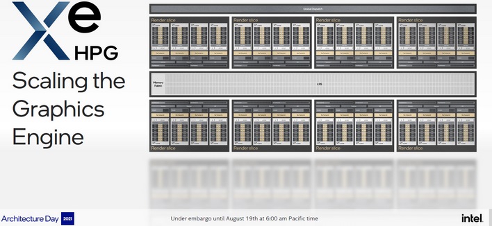
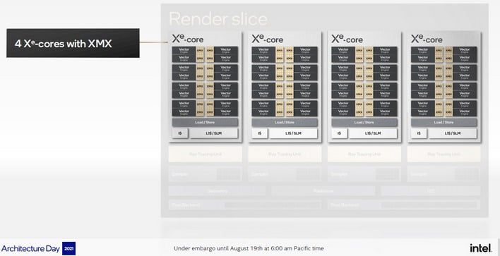
- Up to 8 render slices per GPU instantiation, with 4 cores per slice and 16 vector engines per core. If we do the math, that’s 512 vector engines in a fully populated Alchemist GPU – aka Alchemist/DG2-512.
- Alchemist has 1 ray tracing unit per core and 4 per slice, so that’s 32 RT engines on a full fat Alchemist GPU. If we map that to NVIDIA’s GeForce RTX 30 series, that’s somewhere in between an RTX 3070 at 46 RT cores and RTX 3060 at 28 RT cores, though we’d caution that all RT cores are likely not created equal of course. These RT units support both Microsoft DXR and Vulkan Ray Tracing.
- Intel is claiming a 1.5X clock speed and performance-per-watt uplift versus its XE-LP architecture found in Tiger Lake.
- Alchemist is built on TSMC’s N6 process node, which is a marginal improvement over N7 in terms of transistor density, but certainly competitive with AMD’s and NVIDIA’s current TSMC manufacturing fab process alignments.
Enter XeSS - Intel's Open Source AI-Power Super Resolution Mojo
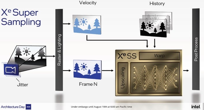
The Intel Arc GPU architecture supports some sort of sweet-sounding, AI-accelerated video enhancement technology capable of high-quality upscaling 480p video content to 4K resolution, but the company didn’t delve into that and instead focused its pitch on XeSS. The “e” here is actually super-script, though the company tends to waffle on lower case or super-script with respect to Xe Graphics. Regardless, XeSS is sort of the best of both worlds of in-game performance reclaiming, as the technology is open source and also can function on legacy Intel and competitive some GPUs. However, XeSS makes use of AI neural network processing on neighboring pixels to reconstruct and upscale cleaner image edge and texture detail from lower resolution game engine input frames.
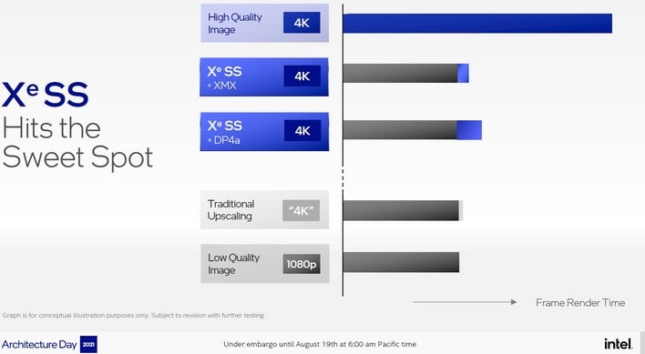
Intel claims the technology can deliver up to a 2X performance boost with Alchemist's built-in XMX AI acceleration hardware that is design to support it, but can also still work on legacy and competitive GPUs leveraging the DP4a instruction set, which can be found in Intel DLBoost technology for AI acceleration as well as NVIDIA CUDA. We believe AMD's RDNA2 GPU architecture can support DP4a instructions as well, so it looks like at least current-gen Radeon hardware may work with the tech.
Regardless, we’re eager to see how XeSS is received in the developer community, and Intel notes its XMX AI Accelerator SDK will be available to game devs this month, with DP4a support later this year. Good game developer adoption of XeSS is going to be critical for Intel’s Arc roll-out. So this will be something to watch for sure.
Now let's dig in to the major Intel Architecture day disclosures for the big iron data center, cloud computing and HPC markets. Right this way...

