NVIDIA GeForce GTX 770 Review With Gigabyte & MSI
It was just last week that NVIDIA launched the seriously potent GeForce GTX 780, which is essentially a scaled-back GeForce GTX Titan, at much more palatable—but still relatively high—price. NVIDIA is not quite done making news, however. As is typically the case when NVIDIA launches a graphics card in a new product family, derivatives that continue to flesh out the product stack are soon to follow. First came the GeForce GTX 780 and today marks the arrival of its little brother, the GeForce GTX 770.
The GeForce GTX 770 looks much like the GTX 780 and Titan, but underneath its cooler assembly lies a different sort of animal, though it’s an animal many of you will likely be familiar with. Take a gander at the specification and glamour shots below and then we’ll fill in the rest of the juicy details on the pages ahead...
|
| Graphics Processing Clusters | 4 |
| Streaming Multiprocessors | 8 |
| CUDA Cores (single precision) | 1536 |
| CUDA Cores (double precision) | -- |
| Texture Units | 128 |
| ROP Units | 32 |
| Base Clock | 1046 MHz |
| Boost Clock | 1085 MHz |
| Memory Clock (Data rate) | 7010 MHz |
| L2 Cache Size | 512 KB |
| Total Video Memory | 2048MB or 4096MB GDDR5 |
| Memory Interface | 256-bit |
| Total Memory Bandwidth | 224.3 GB/s |
| Texture Filtering Rate (Bilinear) | 133.9 GigaTexels/sec |
| Fabrication Process | 28 nm |
| Transistor Count | 3.54 Billion |
| Connectors |
2 x Dual-Link DVI |
| Form Factor | Dual Slot |
| Power Connectors | One 8-pin and one 6-pin |
| Recommended Power Supply | 600 Watts |
| Thermal Design Power (TDP) | 230 Watts |
| Thermal Threshold | 95°C |
| Currently Selling: | $399 on Amazon |
If you’ve been on top of the GPU scene lately, many of the numbers on the chart above will be immediately recognizable. The CUDA core and transistor counts alone allude to the fact that the GeForce GTX 770 is built around NVIDIA’s GK104 GPU, the very same chip that powers the GeForce GTX 680, among some other cards.
Although the GeForce GTX 770 used the same power plant as the GeForce GTX 680, there are some significant differences between the two cards. First and foremost, all GeForce GTX 770s will ship with 7Gbps memory modules, which is the highest clocked GDDR5 memory we have seen. Peak memory bandwidth at that speed is 224.3GB/sec, or about 15% more memory bandwidth than the GeForce GTX 680. We should also point out that NVIDIA’s board partners will offer the GeForce GTX 770 in two configurations, one with 2GB and a higher end model with 4GB, for users targeting ultra HD resolutions.
GeForce GTX 770 also features the same GPU Boost 2.0 technology used in GeForce GTX TITAN and GTX 780, which gives users more advanced controls for overclocking, fan control, and hardware monitoring. The base clock speed of the GeForce GTX 770 reference board is also somewhat higher at 1046MHz, with typical Boost clock speeds is 1085MHz range. At those clocks, the card offers a peak texture filtering rate of 133.9 GTexels/s, up from 128.8 on the 680.
All of that adds up to a card with more features than the GeForce GTX 680, with a better cooling solution, and ultimately higher performance. Some parts of the GeForce GTX 770 are recycled from the 680, of course, but this is not a straight-up re-brand as we’re sure some folks are going to suggest today.
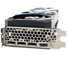
As a final point of referent, the GeForce GTX 770 reference board measures 10.5” in length and requires two-slots to accommodate its double-wide cooling solution, which happens to feature the same vapor chamber and fan design at the GTX Titan and 780. Display outputs on the card include two dual-link DVIs, one HDMI and one DisplayPort connector. One 8-pin PCIe power connector and one 6-pin PCIe power connector are required for operation.


