NVIDIA GeForce GTX 670 Reviews, EVGA and Gigabyte
The new GeForce GTX 670’s features and specifications are very similar to the more expensive GeForce GTX 680 that launched a few weeks back. The two cards feature the very same GPU and similar amounts of memory (4GB versions of both cards are also coming), but a single SMX (streaming multiprocessor) has been disabled in the GeForce GTX 670, which results in fewer total CUDA cores and active texture units.
;)
If you recall, the GeForce GTX 680 has four Graphics Processing Clusters, with eight SMXes, 1536 CUDA cores, 128 texture units, and 32 ROPs. But because a single SMX is disabled in the GeForce GTX 670, it has “only” 1344 CUDA cores and 112 texture units.
In terms of its GPU clock speeds, the GeForce GTX 670 is also slightly scaled back from the GeForce GTX 680. Whereas the GeForce GTX 680 reference specifications call for a 1006MHz base clock and ~1058MHz boost clock, the GeForce GTX 670’s reference specs call for a 915 MHz base clock and ~980 MHz boost clock. The decrease in texture units and frequencies versus the GTX 680 result in a slightly lower 102.5 GigaTexels/sec texture fillrate (bilinear) for the GeForce GTX 670.
;)
;)
;)
;)
As we’ve mentioned, the GeForce GTX 670 also has a shorter board design. NVIDIA moved the power delivery circuitry to the “west” end of the PCB and rotated the GPU to minimize necessary real-estate, which allowed them to shave a few inches off the reference PCB. Although cards are 9.5” long due to the cooler design, the actual PCB is less than 7” in length. Although, we should point out that some board partners have opted to use the same PCB as the GTX 680 with their GTX 670 cards. The TDP is reduced on the GeForce GTX 670 too; it’s down to 170 watts vs. 195 watts for the GTX 680, but a pair of 6-pin supplemental power feeds are still necessary.
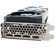
Other than the disabled SMX, lower GPU clocks, and shorter PCB, however, the GeForce GTX 670 is essentially the same as a GeForce GTX 680. The GeForce GTX 670 has the same 256-bit memory interface and its memory runs at the same 6008MHz effective data rate (192.2 GB/s). Outputs on the GeForce GTX 670 also consist of a pair of DVI ports, a mini-DP, and an HDMI output.