Inside Intel Tech Tour 2025: Panther Lake And Clearwater Forest Built On 18A

Intel 18A: Touring Intel’s Ocatillo Campus
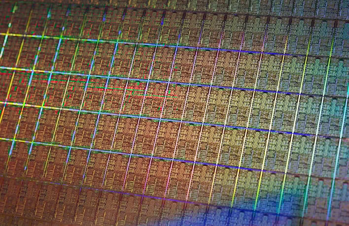
We weren’t allowed to take any pictures and video during our fab tours on the Ocatillo campus, but wanted to spend some time trying to give you a sense of scale at this plant, and drive home the point that Intel is arguably manufacturing some of the world’s most advanced chips right here in the U.S. – TODAY.
Intel’s Ocatillo campus is situated on more than 700 acres of land and features a multitude of buildings and facilities. There are multiple wafer fabrication plants on-site, utility buildings that house chillers and boilers, and wastewater treatment plants, and a multitude of other buildings with everything from cafés to emergency generators. To read or hear news about Intel’s Ocatillo campus is one thing, but to experience in person is something entirely different. The Ocatillo campus is essentially a village or small city. It is huge.
The buildings are all intertwined and leverage shared systems that are critical to manufacturing chips of all types. The focus of our tour was 18A, so we donned our bunny suits, walked through a couple of advanced clean rooms and got to see the fab in action. Although the transistors manufactured on 18A are some of the smallest in the world, everything in the fab is big. Even the size of the ASML High-NA EUV lithography tools dwarf the older EUV tools. The size of the facility has to be seen first-hand to be appreciated.
At the scale Intel requires, the massive footprint and resource requirements of the Ocatillo campus are difficult to fathom. Intel has a webpage available detailing some of the power and water consumption details and other environmental considerations and if you check it out, you’ll see what I mean. But what’s equally interesting is that Intel has put in a ton of work to ensure the surrounding communities are minimally impacted. The campus generates millions of kilowatt-hours of electricity from solar panels, which it pumps out into the local grid as well. It's also equipped with waste-water reclamation facilities, and only 4% of the waste generated actually makes it to the landfill.
Exploring Panther Lake: CPU Architecture Deep Dive

At this point, if you follow the processor space at all, you’re probably well aware of what Intel’s Panther Lake is all about – we’ve been talking about it and posting leaks and other info, including numerous pictures of the chips, for well over a year. To summarize Intel’s official messaging on Panther Lake though, it’s an evolution of Lunar Lake that leverages Intel’s advanced 18A process technology, with more flexible memory configurations, designed to scale performance and efficiency across all its processing engines (CPU, NPU, IPU, GPU).

Like the last few processor generations, Panther Lake is a disaggregated design, composed of multiple tiles, that all happen to be manufactured on different processes, linked together via a base die on a single package using Intel’s advanced Foveros-S 2.5D packaging technology. The compute tile, which is home to the CPU cores and media engine, is built on Intel’s advanced 18A process, the GPU tile is built on Intel 3 or by TSMC, depending on the particular configuration, and the platform controller tile is also manufactured at TSMC.
Although the primary market for Panther Lake will be next-generation AI laptops, it will appear in a variety of designs and form factors, at a myriad of price points, from robots and point of sale systems, to computer vision systems and edge AI IoT devices.


8 And 16-Core Intel Panther Lake CPU Variants
Out of the gate there will be three main Panther Lake chip configurations, an 8 CPU core variant (4P, 4LPE) with a 4-core GPU tile, a 16 CPU core variant (4P, 8E, 4LPE) with the same 4-core GPU tile, and a top-end 16 CPU core model (also 4P, 8E, 4LPE) with a much higher performing 12-core GPU tile. The platform controller tile on all three configuration is mostly similar, and offers up to 20 PCIe lanes (8x Gen 4, 12x Gen 5), 4x Thunderbolt 4 posts, 10x USB ports – split between USB 2 (8x) and USB 3.2 (2x), Wi-Fi 7, and Bluetooth Core 6.0. The only real difference between the platform controller tiles is that all 20 lanes are available on the mid-level 16-core Panther Lake configuration, while only 12 lanes are available on the entry-level 8-core and top 16-core / 12-Xe3 models.


The three main Panther Lake chip configurations also differ in terms of their memory support. The 8-core model can use either DDR5 or LPDDR5X memory, at speeds up to 6,400MT/s or 6,800MT’s, respectively. The mid-level 16 core model will use DDR5 or LPDDR5X memory, but at speeds up to 7,200MT/s or 8,533MT/s. And the top-end 16-core / 12-Xe3 model will use 9,600MT/s LPDDR5X memory only. Intel actually has a strict requirement in place to pair the 16-core / 12-Xe3 variant with only 9,600MT/s memory, to ensure maximum performance, though that memory can be soldered down on the PCB or use LPCAMM modules. We should also note that the maximum memory capacity for the 8 and 16-core models is 128GB, but the 16-core / 12-Xe3 tops out at 96GB.

Panther Lake CPU Core Upgrades: Cougar Cove And Darkmont Unveiled
Panther Lake leverages Intel’s latest CPU core designs. The “big” high-performance P-cores are based on Cougar Cove and the “small” power-efficient E- and LPE-cores are based on Darkmont. At their foundations, theses are not totally new CPU core microarchitectures – Cougar Cove is an evolution of Lion Cove and Darkmont is an evolution of Skymont – but they are both optimized for 18A and feature IPC improvements and offer increased performance over previous-gen designs at lower power. Intel is claiming up to 10% better single-thread performance, with 50% better multi-thread performance at similar power levels to Lunar Lake, or similar MT performance at 30% lower power. With the top end 12-Xe3 core GPU model, Intel is also claiming and 50% more GPU performance.
The width or depth of Cougar Cove is unchanged versus the previous-gen Lion Cove, but there have been enhancements made to improve performance and efficiency. Panther Lake will have 16MB of L2 and up to 18MB of L3 cache, which is a huge, 50% improvement, along with improved heuristics, an updated thread director, and more intelligent AI based power management.
There are also TLB enhancements with 1.5X the capacity for modern workloads. Improved branch prediction, and using the advanced 18A process gave intel the ability to grow some internal structures to reduce latency. The Branch Prediction Unit has been refactored for efficiency as well, and has improved accuracy, lower latency, and more prediction bandwidth over Lunar Lake.

Darkmont, however, is wider and deeper than Skymont, and offers 26 dispatch ports, more vector throughout, more L2 bandwidth, improved nanocode performance, and better, dynamic AI based prefetching like the P-cores – the design can essentially decide if it wants to do more or less perfecting using intelligent algorithms, depending on the workload being run at the time.
The Darkmont cores are arranged in two clusters, with up to 8 standard E-cores and 4-LPE cores – the microarchitecture is the same for both E and LPE cores.

Versus Lunar Lake, the LPE cluster is a big upgrade, and it now features 4MB of shared L2 cache. The LPE cluster not only offers more performance, but it supports a wider range of tasks over Lunar Lake, while maintaining low power. Panther Lake also adds a memory side cache, with 8MB of physical cache, to reduced DRAM traffic, which in turn reduces power, enhances latency, and provides additional caching for the IO engines. The 8 standard E-cores also reside on the L3 cache ring, which is not the case on Lunar Lake.
Intel Thread Director And Power Optimization Revamped For Panther Lake

Due to all of the improvements made across the various CPU cores, Intel also revamped Thread Director in Panther Lake. If you recall, Thread Director essentially classifies the LPE, E, and P-core capabilities and provides dynamic, real-time feedback tables to the operating system. The feedback table updates dynamically based on the particular workloads that are in-flight, to optimize scheduling decisions. On Panther lake, Thread Directors algos are enhanced and optimized to provide better thread guidance across a wider set of modern use cases. Intel optimized the core classification modules to better determine which workload should be dispatched to a particular type of core, and also improved power management input, and expanded busy use case coverage. Panther Lake’s design also allows for simultaneous execution across P, E, and LPE cores.
Because the E and LPE cores are more performant in Panther Lake, efficiency is paramount, and Thread Director will generally start with the most efficient LPE cores if the work fits, and if the workload exceeds the capacity, Thread Director moves on to the E-cores, or ultimately to P-cores.
Intel’s focus on efficiency with Panther Lake also results in some changes to how OS power modes work. Panther Lake will offer what Intel calls an Intelligent Experience Optimizer, which is composed of multiple firmware and software enhancements. Though the traditional power mode slider in Windows will function similarly, if a system is set to Balanced, the Intelligent Experience Optimizer will automatically lean towards offering more performance depending on the workload, but when it detects the need for more efficiency, it will move in that direction. Intel improved the telemetry for the SoC so it can make better power management decisions. Those algos also move from software to hardware for tighter, more responsive control and to offer a more consistent unplugged versus wall-powered experience. Intel claims these dynamic optimizations will help close the AC / DC power delta we typically see on x86 based notebooks and offer an approximate 19% uplift versus baseline DC performance.