Intel Teases Major Speed And Efficiency Gains For 18A Node On Panther Lake

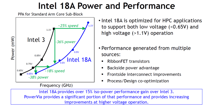
The name 18A is short for 18 angstroms. This is Intel's most advanced node yet, and it represents a major architectural shift. Intel is bringing a number of firsts to 18A, but the biggest ones are RibbonFET, Intel's version of gate-all-around transistors (GAAFET), and PowerVia, the world's first implementation of a backside power delivery network. All of it adds up to a process that, according to Intel, delivers up to 25% higher clocks at the same voltage, or up to 38% lower power at the same performance compared to Intel 3.
Those are wild numbers, especially for ultra-mobile designs where every milliwatt counts, although it's worth noting that Intel never released any consumer products on Intel 3. In fact, the only chips to ever be manufactured on Intel 3 thus far have been the compute tiles for Intel's extant Xeon 6 (codenamed "Granite Rapids") processors.
Intel apparently emphasized that 18A has been optimized for both high performance computing and ultra-low-voltage applications, which is a little unusual given that fabrication process nodes are usually optimized for high-power or low-voltage operation. However, that versatility could be key in securing manufacturing partners for Intel Foundry Services.

Intel has also confirmed that Panther Lake will be the first product to use 18A in volume, ahead of Clearwater Forest for servers. That tracks with Intel's more aggressive roadmap cadence and its desire to reclaim leadership in client CPUs. If you've been following our earlier coverage, you'll remember TechInsights rated Intel 18A ahead of both Samsung SF2 and TSMC N2 in performance-per-watt—a strong sign that Intel's foundry bets might finally be paying off.

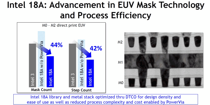
Another interesting tidbit from VLSI 2025: 18A isn't just a one-size-fits-all solution. Intel's offering multiple metal stack variants, including a performance option with 22 metal layers. Combine that with the reduced EUV mask steps—down by 44% versus the previous generation—and Intel seems to have pulled off something that's not just fast and efficient, but also more scalable and cost-effective for production.
The bottom line is that, if Intel delivers on these promises, Panther Lake on 18A could mark a turning point for its mobile division, delivering top-shelf efficiency and performance. We'll be keeping a close eye on samples and silicon leaks in the coming months. The first wave of 18A products should hit late this year, with initial offerings showing up early next year. HardwareLUXX has additional technical details about the advancements in Intel 18A if you're curious to read the nitty-gritty.
