

AMD EPYC 9006 Venice Unveiled: Inside The Zen 6 Architecture

AMD EPYC 9006 Zen 6 Venice Processors: Wider, Deeper, Faster And Higher Density

| AMD EPYC 9006 Processors: Pricing TBD AMD's Zen 6-powered EPYC 9006 Venice processors deliver up to 256 cores, major architectural enhancements, and massive gains in memory and I/O bandwidth. Here's a deep dive into the technology driving AMD's next generation of server CPUs for AI and enterprise workloads. |
|||

|

|
||
A few days ago in Las Vegas, Nevada, at the AMD In Depth event, the chipmaker disclosed many more details regarding its Zen 6 microarchitecture and the EPYC 9006 family of server processors based on it, codenamed Venice. To date, AMD had been fairly vocal regarding Venice and the EPYC 9006 family, but hadn’t revealed all of the speeds and feeds nor the inner-workings of Zen 6—until now. We were able to attend AMD In Depth, so let's dive into everything revealed at the event about these new data center CPUs and the Zen 6 architecture that powers them.

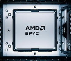
Before we get to the new details, a bit of review is in order. AMD EPYC 9006 Series processors will come in multiple variants, and use multiple sockets, all featuring either Zen 6 or Zen 6c cores, and ranging all the way from 8 to 256 CPU cores (16 – 512 threads per socket). The processors will also come in versions with and without 3D V-Cache for up to 1152 MB of total L3 cache in a single socket, and additional chips (codenamed Verano) are lower-power variants that will leverage LPDDR5X memory. All of the processors will be branded "EPYC 9006," though; they'll be further differentiated based on specific model numbers.

AMD EPYC 9006 Processors: What You Need To Know
EPYC 9006 SP7 is the core of the processor family. These are the densest EPYC chips, with up to 256 cores per socket and up to 5 GHz clock rates, although the 256-core models will use Zen 6c dense cores. Higher-clocked chips, which can reach up to 5.3 GHz will use the bigger Zen 6 cores (sometimes called "classic" cores), with up to 96 in a single socket. TDPs for SP7 CPUs will scale from 400 watts up to 600 watts; SP8 from 130 watts to 400 watts. All of these chips offer 16-channel memory configurations, with your choice of DDR5 RDIMMs at up to 8 GT/s, or DDR5 MRDIMMs at up to 12.8 GT/s. These processors also come with up to 128 lanes of PCI Express Gen 6, and they support additional memory expansion via CXL 3.1.
EPYC 9006 SP8 processors scale things back somewhat. AMD describes them as being "built for efficient, right-sized performance". These are smaller parts, much like the EPYC 8004 "Siena" family that came before, intended for edge compute and more power-constrained environments, or simply anyone who wants a latest-generation EPYC chip and all that entails, yet doesn't need all the cores or connectivity of the big iron. These parts come with between 8 and 128 CPU cores.

Alternatively, for those that need more than the regular EPYC 9006 parts, there's EPYC 9006X SP7. As the “X” branding suggests, these chips will be equipped with AMD's 3D V-Cache. AMD says these parts are made for HPC, technical computing, and data-intensive workloads that benefit from increased L3 cache sizes and higher cache and memory bandwidth. Given that these parts have all the capabilities of a standard EPYC 9006 SP7 plus triple the L3 cache per core, these could be considered the top-end offerings, although not all workloads benefit from 3D V-Cache.
Finally, for more power constrained environments, the EPYC 9006 LP (codenamed "Verano") parts are purpose built to serve as AI host node CPUs for rack-scale AI systems. EPYC 9006 LP processors use LPDDR5X memory—up to 24 channels, with field-replaceable SOCAMM2 modules, providing immense memory bandwidth with lower power than typical DDR5 memory. Like the Venice chips, Verano also supports Unified Power Provisioning, Utilization-Based Power Scaling, and Frequency-Adaptive Spectrum Technology to help with power management and quality of service features.
AMD Zen 6 Microarchitecture Deep Dive

As we’ve mentioned previously, EPYC 9006 processors will make use of both the Zen 6 and Zen 6c microarchitectures. The two core types are mostly identical; they both support the same architecture, ISA, and feature set, and don’t require any specialized software optimization between the two. However, they address different market segments and performance targets. Zen 6c is optimized for density and requires less silicon area per core, whereas Zen 6 is optimized for higher frequencies. The dense Zen 6c cores lose accommodations for 3D V-Cache and sacrifice some frequency versus Zen 6 'classic' to pack more cores into a tighter silicon area.
Like Zen 5, the Zen 6 microarchitecture has a two-basic-block fetch and pipeline, with 8-wide dispatch / rename capabilities. It also features 6 ALUs and support for 4 loads / 2 stores, with a 512-bit floating point data path that supports 2-cycle FADD, along with a 48K L1 data cache. Other improvements to the microarchitecture include a larger µop cache, larger return address stack, larger floating point and integer schedulers, larger load / store queues and a larger re-order buffer. Zen 6 also features increased µop fusion, enhanced branch prediction (with lower misprediction latency), and four VNNI INT8 pipes for AI workloads.

Actual tweaks to the branch predictor block include, optimized branch prediction tables, with a larger 64 entry return address stack. There are also larger branch prediction queues to keep the window growing, with 2 taken predictions per cycle, at up to 3 prediction windows per cycle. The front end also supports a 64B per cycle fetch, optimized for 2 instruction fetch streams. Zen 6 has a larger 6.75K (versus 6K in Zen 5) µop cache as well. All told, the microarchitecture supports a maximum 18 µop delivery per cycle.

Zen 6’s scheduler and execution block supports 8-wide rename and retire, with integer scheduler advances that include distributed schedulers with more total capacity. The design features 96 shared ALUs / AGUs, and 48 dedicated ALUs, versus 88 total in Zen 5. The execution window also grows with a larger 352 entry physical register file and 640 reorder buffer entries.

The microarchitecture features a 48K 12-way L1 data cache with 4 cycle loads, in addition to 4 load / store pipes offering a mix of 4 loads and 2 stores per cycle, with 64B fill / victim to and from the L2 cache, and 4 × 256-bit load support. The Translation Lookaside Buffer is 96 entries and fully associative, with support for all page sizes in the L1 data TLB; the L2 DTLB supports 4,096 entries with memory page sizes up to, but not including, 1G. Zen 6 also has a larger in-flight window; the load queue has grown to 80 entries and the store queue has grown to 128 entries. The load ordering queue is scalable too, and data prefetching has been optimized to better handle larger thread counts.

On the 32-core core complex die (CCD), each Zen 6c core features 1MB of dedicated L2 cache, with 128MB of 16-way L3 shared among all 32 cores in the complex. (Note: There are actually 33 cores in the CCD, to help AMD with die harvesting, but only 32 will ever be enabled.) The L3 is filled from L2 victims (mostly exclusive), and L2 tags are duplicated in L3 for probe filtering and fast cache transfer. 127 outstanding misses are supported from L2 to L3 per core, and 1,280 outstanding misses are supported from L3 to main memory.
Versus Zen 5c, Zen 6c allows for two core complexes per die, with double the L3 cache per core, 4× the total L3 cache, and higher maximum frequencies up to 4.1GHz. Having more cores per CCD also means the maximum core count per socket increases to 256 (up from 192 in Turin).
The standard Zen 6 CCDs also have more cores and support higher frequencies than Zen 5. A Zen 6 CCD moves from 8 to 12 cores per compute complex with a max frequency of up to 5.3GHz (up from 5GHz). There’s the same amount of L3 cache per core, but more total L3 because of the increased core count, resulting in 48MB per CCD. The maximum number of classic cores per socket increases to 96, up from 64 with Zen 5.
Zen 6c is optimized for maximum socket throughput and density, while Zen 6 is optimized for peak core performance and the lowest latency. There are no ISA differences between the two, however, and AMD claims there are no edge cases where Zen 6c and Zen 6 cores behave differently. Due to design differences, they scale differently in terms of performance, power and area, but they are not distinct microarchitectures that require disparate software optimizations, unlike a heterogeneous design.
AMD Zen 6 ISA Updates Bring Gains In Performance And Efficiency

Zen 6 also adds support for a number of new instructions and additional features, as outlined in the slide above. There’s full FP16 support, additional INT8 instructions, instructions to convert BF16 and FP16 data types to FP32, and new Bit Matrix Multiply instructions, among other virtualization and security related features. SEV-SNP, which is an enhanced SMT protection instruction, is interesting because it should result in higher CPU utilization and efficiency, and potentially better performance with some workloads. On previous architectures, unsecure threads were simply prevented from running on the same core as secured threads, but Zen 6 is more intelligent and is capable of running related threads with the same security level on the same cores to take better advantage of SMT and CPU resources.

Comparing queue sizes of Zen 5c vs Zen 6c reveals that the return address stack is increased to 64 from 52. There’s that aforementioned 6.75K µop cache in Zen 6 (vs 6K) and µop cache bandwidth is increased to 18 µops from 12. Integer schedulers are also split and shared in Zen 6 versus unified in Zen 5, the AGU scheduler is now composed of 96 shared and 48 dedicated units versus a total of 88, the integer physical register file is up to 352 entries from 240, the load queue is increased to 80 from 64, and the store queue is increased to 128 from 96.

According to AMD, Zen 6c performs roughly 20% better than Zen 5 with a geomean of enterprise and cloud sever workloads. With AI workloads, the increase is more dramatic: about 31% in testing with similar 16-core counts. Note that 16 cores required 2 CCDs with Zen 5, but only one with Zen 6c. All told, Zen 6 is about 27% better overall across all workloads versus the previous-gen.
Other updates to the SoC and platform include support for PCIe Gen 6 with CXL 3.1, a 5th generation Infinity Fabric with faster fabric p-state changes, elevated fanout bridges (EF8) for die-to-die communications, and significantly lower pJ/b (picojoules per bit) for more efficient data transfers, which also affords more power per CPU core. The processors support both 1P and 2P socket configurations like previous-gen parts too, but bandwidth between the sockets has been doubled, with up to 3 links of 64Gbps Gen 5 Infinity Fabric divided amongst the sockets.

The design and chiplet structure of the processors is mostly similar to previous-gen EPYC processors, but the microarchitectural differences result in vastly different product stacks. EPYC 9006 series processors will have up to 8 CCDs per CPU, for up to 256 Zen 6c cores or up to 96 Zen 6 cores. There are also two IO dies per processor on the SP7 platform offerings, each with 8× DDR5 memory channels, for a total of 16 channels, with peak theoretical bandwidth of 1.6TB/s per socket (16 channels × 8B × 12.8 GT/s). That equates to up to 2.6× higher memory bandwidth using JEDEC standard DIMMs versus previous-gen EPYC platforms. Peak IO bandwidth also doubles thanks to PCIe Gen 6. Each IOD has 48 lanes of 64G SerDes and 8 lanes of 16G SerDes, for a total of 96L of 64G SerDes and 16L of 16G SerDes due to the dual IOD design.

The EPYC 9006 Venice SP8 platform has a somewhat different I/O configuration. EPYC 9006 processors for the SP8 socket will have a new IO die with a different number of memory channels and different PCIe Gen 6 lane configuration. SP8 has half the memory channels (hence half the bandwidth and max capacity), but more PCIe Gen 6 lanes, up to 128 lanes in this case, with 8 additional Gen 4 lanes.
Which brings us to Verano, the EPYC 9006 LP series. Verano will feature up to six 32-core Zen 6c CCDs (192 total cores) or 6 12-core Zen 6 CCDs (72 total cores), but with the addition of what AMD is calling “memory winglets” to support LPDDR5 memory. EPYC 9006 LP “Verano” processors offer essentially all of the benefits of Venice SP7, but with support for lower power memory in a different socket infrastructure, designed for optimal power efficiency. Memory is a significant factor in uncore power, so moving to LPDDR saves significant total power at the cost of increased memory latency.
AMD MEXT Could Help Mitigate The Current Memory Crisis

Another memory-related technology coming with EPYC 9006 is MEXT. AMD MEXT is the product of a recent acquisition that could help customers maximize TCO by better optimizing the amount of physical memory (DRAM) required for their particular use cases.

MEXT is an AI-driven memory optimization technology that makes use of NVMe flash storage to act somewhat like an additional memory tier. MEXT allows the flash memory to behave more like system memory, expanding a system's total effective memory capacity, to better handle memory-hungry workloads.

Instead of relying solely on expensive DRAM, MEXT moves less-active data to flash storage and uses predictive AI algorithms to anticipate which data will be needed next, proactively bringing it back into DRAM before applications request it. Memory pages that go cold (which aren't accessed for multiple minutes) are shuffled off to the NAND, and proprietary AI algos predictively retrieve those cold pages just before their needed.

AMD says that this approach can effectively expand available memory, improve infrastructure utilization, and lower memory-related costs while maintaining application performance for workloads like AI, analytics, simulation, and large-scale data processing. MEXT is a software solution that is fully configuration based on the customers' needs. AMD is releasing a memory analyzer tool, dubbed RAM View, to help customers determine proper optimization points, which could effectively boost memory capacity by 2x or more.
For now MEXT is exclusive to the EPYC 9006 platform, but the technology has to much promise to stay locked to AMD's server platform indefinitely. MEXT's impact on local AI with devices like the Ryzen AI Halo could be significant, so we expect it to migrate to other platforms in the future.
AMD Zen 6 And The EPYC 9006 Series Conclusions
Throughout the presentations at AMD In Depth, engineers and company leadership underscored that EPYC 9006 platform is laying the foundation for future architectures. Obviously, we’re not privy to any concrete Zen 7 details just yet, but Zen 6 is here today and it seems AMD made a number of strategic bets that should pay dividends as we head into the agentic AI era. With EPYC 9006, not only is the company offering its most performant and densest server CPU platforms yet, but it’s got a deep, diverse set of products in the portfolio to address a wide range of market needs, from maximum density with dual 256C/512T processors in a 2P platform, to lower power offerings with immense I/O capabilities that leverage LPDDR5 memory.Agentic AI is causing demand for CPUs to surge once again, and despite increased competition from NVIDIA and Arm, and soon Intel with Diamond Rapids, AMD seems very well positioned to capitalize on the trend. With Zen 6 and the EPYC 9006 series of products, AMD ticks many of the right boxes. From increased density, to higher per-core performance, more memory bandwidth and memory capacity, lower-power platforms, and massive cache sizes, EPYC 9006 seemingly has something for every data center application.