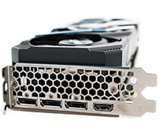
GeForce GTX 275 and Radeon HD 4890 Round-Up
The PC world was treated to one of those rare occurrences a few weeks back--a 1-2 punch into the 3D graphics fray from both ATI and NVIDIA. We're talking about the near simultaneous launches of the ATI Radeon HD 4890 and NVIDIA GeForce GTX 275. Both of their names lead to obvious suggestions about where they fit into their respective families.
With the Radeon HD 4890, one might assume that there was an update made to the venerable HD 4870, and for the most part that assumption would be correct. Both GPUs share the same number of shader processors, texture units, and ROPs, bit with three million more transistors than the RV770, and hence a larger die, clearly something else was at work here. As most of you probably know by now, the Radeon HD 4890 is based on a new GPU dubbed the RV790 and that the additional transistors along with the inclusion of a decap ring that reduces electromagnetic interference gave AMD the ability to raise clock speeds over the 4870 by about 100MHz, give or take a few MHz depending on the model.
Also, as its name suggests, NVIDIA's GeForce GTX 275 fits comfortably into the slot between the GTX 260 and GTX 285 cards, with a price set to match the HD 4890. All three of these cards are powered, for the most part, by NVIDIA's GT200b GPU, but are equipped with varying number of stream processors, different amounts of memory, and differing memory interface widths and ROP configurations. At its most basic level, the GTX 275 is a lower power version of the GTX 285, using the same 55nm die at a clock speed of 633MHz while the GTX 285 runs at 648MHz.
With some of the background now covered, we take a look at seven cards, three Radeon HD 4890s and four GeForce GTX 275s, from some of the most prominent names out there. Which one of these cards deserves your hard-earned dough? Read on and find out...
| Card |
Core Clock |
Shader Clock |
Memory Type and Capacity |
Memory Clock |
Memory Bandwidth |
|
Radeon HD 4890 | |||||
|
|
925 MHz |
N/A |
1GB GDDR5 |
1050 MHz |
134.4 GB/s |
|
|
900 MHz |
N/A |
1GB GDDR5 |
1000 MHz |
128.0 GB/s |
|
|
875 MHz |
N/A |
1GB GDDR5 |
975 MHz |
124.8 GB/s |
|
GeForce GTX 275 | |||||
|
|
633 MHz |
1404 MHz |
896MB GDDR3 |
1134 MHz |
127.0 GB/s |
|
|
633 MHz |
1404 MHz |
1792MB GDDR3 |
1134 MHz |
127.0 GB/s |
|
|
633 MHz |
1404 MHz |
896MB GDDR3 |
1200 MHz |
134.4 GB/s |
|
|
666 MHz |
1476 MHz |
896MB GDDR3 |
1161 MHz |
130.0 GB/s |
Now, there's much more to these cards than the basic specifications that we've shown you here. The chart above is there to show the major difference between the cards, mostly in regards to GPU and memory clock speeds as well as the amounts of memory installed and their respective memory bandwidth. For a more complete rundown of either the RV790 or GT200b architectures, we recommend checking out some of our previous articles including the launch pieces on both the HD 4890 and GTX 275:
With all that reading out of the way, we're set to take a look at our first cards based on ATI's RV790.


