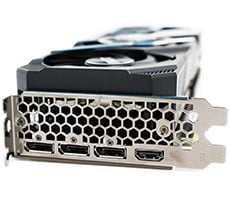
Foxconn GeForce 8800 GTX
Those who are familiar with the GeForce 8800 GTX will instantly recognize the familiar look of NVIDIA's reference design when they glance at Foxconn's card. Given the low noise and cooling performance afforded by the reference design, this was certainly not a bad move on Foxconn's part. Much like nearly all other GeForce 8800 GTX models, Foxconn has used customized graphics on top of the heatsink assembly to help differentiate their products from the others. Turning the card over, it would be nearly impossible to distinguish which vendor's card this was as there are no unique features to provide any clues.
Taking a glimpse at the side of the card, we see the significant size and heatpipes of the dual-slot heatsink assembly. Upon closer investigation, we can see there is a series of LED's which are aligned around the top-most perimeter of the heatsink assembly. Sure enough, once we power the card we find a collection of blue LED's filling the inside of the case with understated lighting which won't trigger any seizures or prove to be too distracting.
As we mentioned in our initial review of the GeForce 8800 GTX, the card features two SLI connectors at the top of the PCB. At this time, only one SLI connector can be used at once though the user can choose either connector. Moving our eyes towards the back of the card, we find two PCI-Express power headers. Unlike the SLI connectors, both must be used in order for the card to receive the appropriate amount of power and function properly.
Much like with all enthusiast hardware, one of the greatest pleasures is taking the product apart and taking a peek beneath the hood. After removing the massive heatsink assembly, we can see how many portions of the card are receiving direct contact with the cooler. With the exception of the thick thermal paste used directly on the GPU, the rest of the components including the memory and NVI0 TMDS logic are cooled using a liberal amount of white thermal tape. After removing the remaining thermal paste from the face of the GPU, we noticed what appeared to be a checkmark of sorts made with a Sharpie marker. With no information regarding the marking, we suspect this is some semblance of "binning" where the higher-quality yields are separated from the rest of the bin which might barely meet required frequencies.
Glancing at the board, we have no less than 12 Samsung GDDR-3 memory chips which are rated to operate at or above the GeForce 8800 GTX's standard 1.8GHz reference memory speed. More uniquely however, we have NVIDIA's TMDS display logic which has traditionally been placed within the GPU itself. However, in order to shave costly die sizes and cut transistor count NVIDIA opted to break this out into a separate physical piece of logic.


