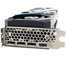
NVIDIA GeForce 8800 GTX and 8800 GTS: Unified Powerhouses
The GeForce 8800 series GPU in a massive piece of silicon. It's comprised of roughly 681 million transistors and manufactured on TSMC's 90nm process node. It implements a massively parallel, unified shader design, consisting of up to 128 individual stream processors in up to 8 groups of 16, running at frequencies of up to 1.35GHz. The GeForce 8800 GTX takes advantage of all 128 stream processors, but the GTS has two blocks disabled for a total of 96 stream processors. And the unified nature of the design means each processor is capable of being dynamically allocated to vertex, pixel, geometry, or physics operations, unlike traditional GPU architectures that feature discreet pixel and vertex shaders.

GeForce 8800 Series GPU Block Diagram
Each GeForce 8800 GPU stream processor is a fully generalized, fully decoupled, scalar, processor that supports IEEE 754 floating point precision. The advantages of being fully scalar, are well summed up in this quote provided by NVIDIA
|
"Although leading GPUs to date have used vector processing units, because many operations in graphics occur with vector data (such as R-G-B-A components operating in pixel shaders or 4x4 matrices for geometry transforms in vertex shaders), many scalar operations also occur. During the early GeForce 8800 architecture design phases, NVIDIA engineers analyzed hundreds of shader programs which showed an increasing use of scalar computations. They realized that with a mix of vector and scalar instructions, especially evident in longer, more complex shaders, it's hard to efficiently utilize all processing units at any given instant with a vector architecture. Scalar computations are difficult to compile and schedule efficiently on a vector pipeline. Both NVIDIA and ATI vector-based GPUs have used shader hardware that permits dual instruction issue. Recent ATI GPUs use a "3+1" design, allowing single issue of a four-element vector instruction, or dual-issue of a three element vector instruction and a scalar instruction. NVIDIA GeForce 6x and GeForce 7x GPUs are more efficient with 3+1 AND 2+2 dual-issue design, but still not as efficient as a GeForce 8800 GPU scalar design, which can issue scalar operations to it's scalar processors with 100% shader processor efficiency. NVIDIA engineers have estimated as much as 2X performance improvement can be realized from a scalar architecture that uses 128 scalar processors versus one that uses 32 4-component vector processors, based on architectural efficiency of the scalar design. (Note that vector-based shader program code is converted to scalar operations inside a GeForce 8800 GPU to ensure complete efficiency.)" |
All of the stream processors in the GPU are driven by a high-speed clock domain that is separate from the core clock that drives the rest of the chip. For example, the GeForce 8800 GTX core clock is 575MHz and its stream processors run at 1.35GHz. The GeForce 8800 GTS has a core clock of 500MHz, but its stream processors are clocked at 1.2GHz.

The GeForce 8800 series GPU also has six memory partitions that each provide a 64-bit interface to memory, yielding a 384-bit combined interface width on the GTX. One of the memory partitions is disabled in the GTS, which yields a 320-bit memory interface. The memory subsystem implements a high-speed crossbar design, similar to GeForce 7x GPUs, and supports DDR1, DDR2, DDR3, GDDR3, and GDDR4 memory. The GeForce 8800 GTX uses GDDR3 memory clocked at 900MHz with a 384-bit (48 byte-wide) memory interface running at 900MHz (1800MHz DDR) - that equates to 86.4GB/sec. Yikes.

Texture filtering units are also fully decoupled from the stream processors. The GeForce 8800 series GPU can deliver up to 64 pixels per clock worth of raw texture filtering horsepower (vs. 24 in GeForce 7900 GTX), 32 pixels per clock worth of texture addressing, 32 pixels per clock of 2X anisotropic filtering, and 32-bilinear-filtered pixels per clock.
The GeForce 8800 GTX has six Raster Operation (ROP) partitions (the GTS has 5). Each partition can process 4 pixels with 16 sub-pixel samples, or a total of 24 pixels/clock with color and Z processing. For Z-only processing, an advanced new technique allows up to 192 samples/clock to be processed when a single sample is used per pixel. If 4x multi-sampled anti-aliasing is enabled, then 48 pixels per clock Z-only processing is possible.

Another new feature inherent to the GeForce 8800 series GPU is dubbed Early Z. Z comparisons for individual pixel data have generally occurred late in the graphics pipeline in the ROP. The problem with evaluating individual pixels in the ROP is that the they have already traversed nearly the entire pipeline. If the pixel ends up being occluded, that's a waste of GPU resources and bandwidth. With complex shader programs that have hundreds or thousands of processing steps, that a lot of processing that can be wasted on pixels that will never be displayed.
To somewhat alleviate this issue the GeForce 8800 employs an Early Z technique test Z values of pixels before they enter the shader pipeline. The result is that a GeForce 8800 GTX GPU can cull pixels at four times the speed of GeForce 7900 GTX.

We'll cover the individual specifications of the new GeForce 8800 GTX and 8800 GTS cards being announced today a little later on, but we thought we'd give you a high level breakdown before discussing some more of the other advanced features offered by NVIDIA latest flagship GPU. Due to the scalable nature of the GPU design, functional blocks can be disable, yielding a GPU with different performance characteristics.


