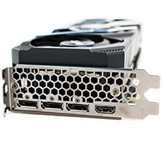
AMD Radeon HD 6970 & 6950 Debut: Enter Cayman
At its core, the GPU codenamed “Cayman” is comprised of 2.64 billion transistors and its die size is roughly 389mm2. If you’re keeping track, Cypress (Radeon HD 5870) was comprised of about 2.1 billion transistors and had a 334mm2 die while NVIDIA’s GF110 is made up of approximately 3 billion transistors. The actual die size for NVIDA’s part hasn’t been disclosed, however, numbers in the 529mm2 range have been thrown around.

Cayman GPU High-Level Block Diagram
Here we have a high-level block diagram of the Radeon HD 6900 series GPU, aka Cayman. This chip is different from the previous generation Radeon HD 5800 series GPU in a number of ways. First and foremost, the 6900 series is outfitted with dual graphics engines which help keep the GPU well-fed with data, whereas the 5800 series had one. The 6900 series GPU also employs a VLIW4 (Very Long Instruction Word) design; the 5800 was a VLIW5 design. In its full configuration, the chip has 24 SIMD engines, 96 texture units, 32 ROPs (which have been upgraded from previous generations), a 256-bit memory interface and a number of enhancements to improve GPU compute features.

The Dual Graphics Engines Up Close
Cayman’s dual graphics engines give the chip the ability to process two primitives per clock and the dual-engine configuration offers double the transform and backface cullrate than the 5800 series. Incorporated into the engines are also the chip’s dual 8th generation tessellators which now have off-chip buffer support for high tessellation levels among other tweaks. AMD claims the new tessellators will perform up to 3x better than the 5870. Dual rasterizers allow the Radeon HD 6900 series GPU to process up to 32 pixels per clock.


The New Core (left) and Render Back End (right) Designs
The new VLIW4 cores have a 4-way co-issue design and all of the cores have equal capabilities. The VLIW5 cores in the 5800 series had a special “T-Unit” that was more capable than the other four units in the core. AMD claims the new core design offers a 10% improvement in performance per mm2 with simplified scheduling and register management.
The render back-ends, or ROPs, have also been upgraded in the 6900 series GPU. The new render back-ends in the chip allow for coalescing of write ops and they can now handle 16-bit integer (unorm/snorm) ops at twice the rate and 32-bit floating point (single/double component) ops are 2x to 4x faster. The end result is faster anti-aliasing performance that causes less of a performance hit than the previous generation.


