AMD A10 and A8 Trinity APU: Virgo Desktop Experience
We’ll be taking a somewhat different two-tiered approach with our coverage of AMD’s new Trinity-based APUs for desktop systems today. AMD is lifting the veil on their new product line-up, in addition to graphics performance and power consumption, but we can’t quite give you the full monty just yet, due to a new multi-tiered launch approach AMD decided to take with these products. If you want to see how well AMD’s latest desktop APUs overclock, how their processor cores perform, or how they’re priced, you’re going to have to stop by in a few more days. For now though, we’ve got graphics performance and power consumption characteristics to talk about and have some rather interesting side-by-side comparisons in store as well.
AMD Trinity APU Die Shot
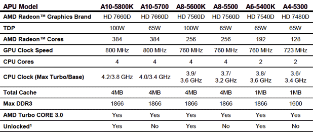
We’ve already shown you what AMD’s Trinity-based APUs can do in their mobile form, but the desktop variants are somewhat different animals. Although they’re based on the same piece of silicon, Trinity-based APUs for desktop systems have much more power and thermal headroom to play with. As such, the chips are clocked much higher, in regard to both their CPU and GPU cores. In fact, one of the chips we’ll be showing you here today, the A10-5800K, can Turbo all the way up to 4.2GHz. Take a look at desktop Trinity’s main features and specifications below and take a few minutes to see how the A10’s GPU performs versus an Intel Core i3 in the video here. We’ll move on to more details and performance data on the pages ahead.
AMD Trinity A10-5800K Piledriver APU vs Intel Core i3 Ivy Bridge Demo
|
- Die size: 246mm2

- 1.303B transistors
- Process: 32nm SOI
- 2.09W MobileMark 07 power consumption
- 1.08W idle power
- Power reduction during HD media playback
- Unified Northbridge (UNB)
- Quad-core and Dual-core configurations
- Updated AMD Radeon™ DirectX®11 GPU
- 3 dedicated display outputs
- 4 independent display controllers
- DisplayPort 1.2 with symbol rates of 1.62, 2.7 and 5.4 Gbit/s
- UVD and AMD Accelerated Video Converter
- IOMMU v2 (Input/Output Memory Management)

As we detailed in our coverage of the mobile variant, AMD's Trinity APUs are comprised of a little over 1.3B transistors and have a die size of 246mm2. If you're keeping track, Intel's Ivy Bridge processors are built from roughly 1.4B transistors with a die size of about ~160mm2. That's the difference between 22nm and 32nm process technology; AMD is still a full process generation behind at the moment.
Though die size is directly proportional to cost, power consumption may or may not be, depending the power gating technologies, architectural enhancements, and leakage currents at play. As you can see in the chart above, Trinity sips barely over 1W of power at idle and the current top-end A10 desktop chips have a 100W TDP with a max clock speeds of 4.2GHz. Beyond that, you can see that AMD is bringing out several versions of their new desktop Trinity-based APUs, with both dual-core and quad-core variants, along with various Radeon HD 7000 series integrated GPUs on board, clocked at different speed bins and varying numbers of active GPU cores.
AMD A10-5800K and A8-5600K Side-by-Side
AMD's lowest power desktop chip is the A4-5300, which is a dual-core CPU with a Radeon HD 7480D graphics engine on board consisting of 128 Radeon cores. Today, however, we'll be showing you all the graphics performance of the high-end A10-5800K and A8-5600K unlocked quad-core parts designed with on-board Radeon HD 7660D and 7560D graphics engines and comprised of 384 and 256 Radeon cores, respectively, running at a peak clock speeds of 800Hz and 760MHz. The CPU cores however, come in at 3.8GHz / 4.2GHz for the A10-5800K and 3.6GHz / 3.9GHz for A8-5600K, taking into account base and maximum turbo speeds.


