Alienware Aurora m9700
So what do you do when you have one of the only Engineering Samples of a brand new notebook platform at your disposal? Within minutes of receiving the system, we had the appropriate panels removed and were taking a closer look under the hood to see what surprises Alienware had in store with this new notebook. Armed with a trusty digital camera, we've documented the disassembly process for your viewing pleasure.
Looking at the bottom of the unit, we see one main panel that covers a large portion of the base. Removing this panel unveils a dense collection of heatsinks and components. Upon first glance, we see two graphics cards, two memory modules, the processor, and a seemingly endless loop of heatpipes and heatsink assemblies. Despite such a concentrated grouping of components, the layout is surprisingly clean and efficient.
After removing the heatsink assemblies, we are able to truly see the overall layout of the board and the orientation of the components. Here, the heatsink assembly used to cool the GPU's serves double duty as it also cools the nForce4 SLI chipset. Although found in a mobile system, this is actually the same chipset used in desktop SLI motherboards. Moving our attention to the right, we find the AMD Turion64 ML-44 processor in all its glory.
One of the most interesting aspects of the Aurora m9700 system's internals would be the use of an SLI bridge card to tell the system whether it is using single or dual GPU's. Common on all first generation desktop SLI boards, these bridge cards have since been replaced by logic that is able to sense the presence of a GPU and configure the system accordingly. We are told that although the 17" Aurora m9700 features a bridge card, the 19" ALX system (made by a different notebook ODM) will not use a bridge card and will instead do everything in logic like nearly all current desktop nForce 4 SLI motherboards. nForce 4 SLIX16 and new nForce 590 SLI based motherboards don't need the bridge because they can feed 16 PCI Express lanes to each PEG slot.
In terms of supporting SLI, there are a number of required components. Looking at the images above, we see that beyond the obvious need for two discrete graphics cards we also need the previously mentioned bridge card as well as a flexible SLI connector. The SLI connectors themselves are surprisingly small as evidenced by the provided image using a finger for scale.
The crown jewels of the Aurora m9700 would certainly be the dual GeForce Go 7900 GS graphics card modules. Based on an MXM3 format, these modules each feature 256MB of memory to accompany the G71 GPU. Specifically, the modules we tested used Infineon memory modules that are rated for 500MHz which is the target operating frequency for this GPU as we will see below.
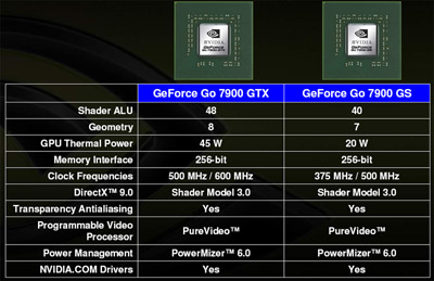
Referencing the appropriate slide from NVIDIA's presentation, we can clearly see the differences between the GeForce Go 7900 GS and the flagship GeForce Go 7900 GTX. Essentially, the GeForce Go 7900 GS has 8 fewer Shader ALU's with a slight disadvantage in terms of Geometry processing. The 125MHz decrease in core frequency and 100MHz lower memory frequency allow the GeForce Go 7900 GS to have a 25W lower power consumption than NVIDIA's flagship mobile part.


