NVIDIA GeForce GTX 980 & 970 Maxwell GPU Reviews
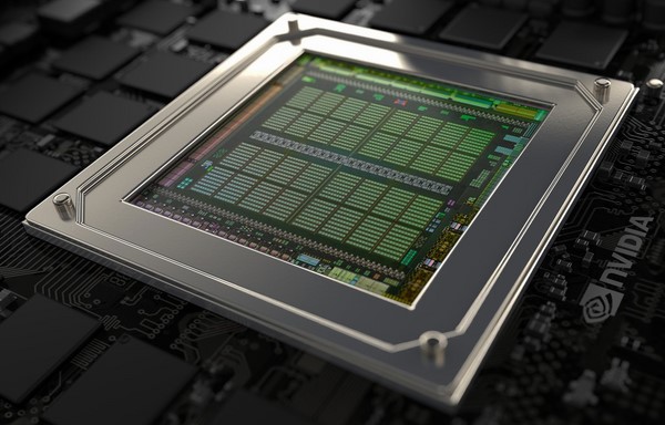
While Maxwell is a new GPU architecture for NVIDIA, these GPUs do not leverage a new manufacturing process. The 5.2 billion transistor GM204 is still built on TSMC’s 28nm process and has an approximate die size of 398mm2. It’s likely that future Maxwell-based GPUs will use a more advanced manufacturing process, but for now, 28nm is it.
NVIDIA was able to optimize the GM204’s power efficiency, however, without moving to a new process, by tweaking virtually every part of the GPU. NVIDIA took what they learned with Kepler and its Tegra SoCs and put much of that knowledge into Maxwell. Maxwell is designed to boost efficiency through better GPU utilization, and ultimately improve performance per watt and per die area. NVIDIA claims that Maxwell SMs (Streaming Multiprocessors) offer double the performance of GK104 and double the perf per watt as well. The scheduler in GM204 has received a number of updates to improve power efficiency, but also enhance performance.
Maxwell’s Streaming Multiprocessors, or SMs, are somewhat different than Kepler’s. With Maxwell, NVIDIA has made improvements to the control logic partitions for better workload balancing, and it also has finer-grained clock-gating and better compiler-based scheduling. Maxwell can also issue more instructions per clock cycle, all of which allow the Maxwell SM (also called an SMM in some NVIDIA docs) to exceed Kepler’s SMX in terms of efficiency. NVIDIA is claiming that Maxwell’s new SM architecture can deliver 40% more performance per CUDA Core on shader-limited workloads than Kepler, with up to double the performance per watt, despite using the same 28nm manufacturing process.
Due to the architectural and SM design differences, NVIDIA was able to increase the number of SMs in GM204 to 16, versus 15 in GK110 and 8 in GK104. NVIDIA also increased the L2 cache size to 2MB versus 1536K in GK110 and 512K in GK104, with only a modest increase in die area. Each SM in the GM204 includes a third-gen Polymorph Engine and Texture Units, while each GPC includes a Raster Engine. And its ROPs are aligned with L2 cache slices and Memory Controller partitions.
The GM204 GPU contains four GPCs, up to 16 Maxwell Streaming Multiprocessors (SM), and four 64-bit memory controller partitions (256-bit total). Each SM is now partitioned into four separate processing blocks, each with its own instruction buffer, scheduler and 32 CUDA cores. With Kepler, the control logic had to route and schedule traffic to 192 CUDA cores, which were harder to keep fully utilized. This partitioning simplifies the design and scheduling logic, saving area and power, and reduces computation latency. The compute L1 cache function has now also been combined with the texture cache function, and shared memory is a separate unit shared across all four blocks.
Maxwell also features an improved NVENC block (Hardware Video Encoder) that provides faster encode (6-8X real-time for H.264 vs. 4x real-time for Kepler) and 8-10X faster decode as well, and thanks to a new local decoder cache, Maxwell has higher memory efficiency per stream for video decoding, which also results in lower power for video decode operations. The updates to the NVENC block make the GM204 a perfect companion to NVIDIA's ShadowPlay feature. We should also point out that Maxwell and the GM204 are ideal for streaming to SHIELD devices as well.
Also new to “Big Maxwell” is a third-generation delta color compression technology. NVIDIA is claiming it can achieve up to an 8:1 compression ratio. The memory architecture also benefits from improved caching effectiveness. Despite offering less peak, total bandwidth than the higher-end GK110 (which has a 384-bit memory interface), the GM204 still performs very well, as you’ll see in a just a bit.


