Intel Clarkdale Core i5 Desktop Processor Debuts
Avid followers of the PC technology scene are no doubt familiar with the concept of CPU + GPU fusion. AMD has been talking about its Fusion project for years, which will feature advanced processor and graphics cores on a single chip. Well, we're not quite there yet, not on the desktop at least, but Intel is taking us one step closer with Clarkdale. Yes, we said Intel.
A couple of weeks ago, we evaluated Intel's Pinetrail platform for netbooks, which features an Atom CPU core, fused to a graphics processor on a single, monolithic die. Today, Intel is taking a similar approach in the desktop space with the company's much more powerful Clarkdale family of processors, although Clarkdale's integrated graphics processor isn't on-die--it is on the same package as the CPU though.
Clarkdale-based processors feature a number of cutting edge Intel technologies. For one, the processor cores are manufactured using a 32nm high-k process. They also feature Intel Turbo Mode technology, Hyper-Threading, AES acceleration, and Intel's latest graphics processing core, branded Intel HD Graphics, that also happens to house a memory controller and PCI Express connectivity.
The Clarkdale architecture will be used for a whole family of new processors in the Core i5, Core i3, and Pentium series. We've had one of the higher-end offerings in house for a few weeks, the Core i5 661, and have been putting it through its paces for most of that time. Read on for the full scoop...

Clarkdale Processor with Integrated Graphics, H57 Chipset
|


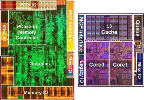
Clarkdale GPU and CPU Dies To Scale
Some may be confused into thinking Clarkdale is simply a die-shrink of Lynnfield with graphics attached, that is actually not the case. As the above image shows, Clarkdale's memory controller and PCI Express lanes are actually integrated into the graphics core, and not the CPU as they are with Lynnfield. Also note, the graphics core is physically larger than the CPU core, even though it is comprised of less than half the number of transistors. This is due to the fact that the graphics core is manufactured at 45nm whereas the CPU is manufactured at 32nm, as we've mentioned. To be more specific, the 32nm CPU die is comprised of 383 Million transistors, and is about 81mm2, while the 45nm graphics die is made up of roughly 177 Million transistors, and is 114mm2.
There's lots more to talk about though. First we'll cover the Core i5 661 and high-level features of Clarkdale, and will move on to the Intel HD Graphics engine, and new chipsets from there...


