Intel 10nm Ice Lake Architecture And Project Athena Laptops To Drive Exciting New Mobile PC Experiences
Over the last few months, Intel has disclosed a number of details regarding its next-generation 10nm processors, codenamed Ice Lake. At an Architecture Day held in December ’18, we learned about the company's Sunny Cove microarchitecture that will be employed in Ice Lake and future-generation processors, in addition to some details regarding Intel’s Gen11 graphics engine.


Ice Lake is the next foundational architecture Intel is introducing into the PC client ecosystem. Like Skylake that came before it, and Haswell before that, the core architecture employed in Ice Lake will be used in an array of processor designs moving forward. The first Ice Lake-based products to arrive will target the mobile market, but the architecture will eventually make its way into Intel’s desktop and other processor segments as well.

According to Intel, every single piece of IP in Ice Lake was affected versus previous-gen architectures. Ice Lake features new transistor technology, a new core graphics engine and additional platform integration. An additional metal layer has been added for better power delivery and the CPU cores themselves leverage a new microarchitecture, dubbed Sunny Cove.
Ice Lake 10th Generation Intel Core processors feature DL Boost (Deep Learning) to accelerate AI workloads, in addition to a new, intelligent Dynamic Tuning algorithm that leverages machine learning to optimize power consumption and performance. Thunderbolt 3 has been integrated into the processors themselves to simplify routing and minimize board real-estate, and Wi-Fi 6 technology capable of greater than Gigabit speeds is part of the platform as well. Finally, Intel's new Gen11 graphics engine features dual HEVC encoders and up to 64 EUs, to boost performance dramatically over Intel’s previous-gen graphics engines.

10th Generation Intel Core mobile processors will feature up to four cores (eight threads with Hyper-Threading) and boost clocks up to 4.1GHz, though future mobile processors with more cores and higher-clocks (in higher power envelopes) are likely to arrive as well. Thunderbolt 3 is integrated into the SoC (more on this later). There is a new, high-bandwidth / low-latency Converged Chassis Fabric linking the cores and various IP around the processor, and a revamped memory controller with support for DDR4 and LPDDR4X also makes its debut. The memory controller can be configured in a 4x32b or 2x64b configuration, when utilizing LPDDR4X or standard DDR4, though the maximum frequency and capacity for each configuration differs greatly. For peak performance, the 3733MHz 4x32b configuration would provide the most bandwidth (roughly 50-60GB/s) and lowest latency, which is of paramount importance to the chip's integrated graphics engine.
Speaking of graphics, the Gen11 graphics engine in Ice Lake can have up to 64 next-gen EUs, clocked at up to 1.1GHz, which in turn offers up to 1.13 TFLOPS of double-precision compute, or 2.25 TFLOPS of FP16. The entire 3D pipeline and memory subsystem has been re-worked to enhance performance and efficiency, it features an improved rasterizer, and can handle 16 pixels per clock or 32 bilinear texels per clock, versus only 12 on the previous generation. A hybrid Tile Based rendering mode is also available for workloads that are bandwidth constrained, which can be optionally enabled when needed.
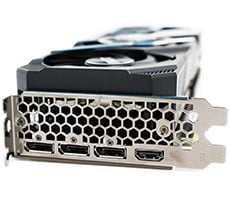
There are dual HEVC encoders on-board, which can be used concurrently for independent workloads or ganged together for higher performance on a single stream. The encoders can handle up to 8K30 4:2:0 when ganged together on a single stream or up to 4K60 4:4:4 with dual streams. Three display pipes are also present, with support for DisplayPort 1.4 HBR3 and HDMI 2.0B, at up to 5K60 or 4K/120 10Bit resolutions. Support for VESA Adaptive Sync, variable refresh rate monitor technology is also available as well.
Sunny Cove Microarchitecture Details

At the heart of Ice Lake’s CPU cores is the new Sunny Cove microarchitecture. We first told you about Sunny Cove back in December after Architecture Day, but have some more details to share with you here. Sunny Cove is wider and deeper than Intel’s previous-generation microarchitecture. It has larger key internal structures and larger caches, to help improve IPC and overall multi-core performance. There are now 5 allocation units (versus 4 previously), 10 execution ports (versus 8), 4 AGUs (versus 3), and double the L1 store bandwidth. Sunny Cove also features a more accurate branch prediction unit. Intel claims Sunny Cove reduces load latency and features a PC client-optimized design as well.

In comparison to Haswell and Skylake, the Sunny Cove microarchitecture used in Ice Lake is enhanced virtually across the board. In addition to the aforementioned features, Sunny Cove has more L1 cache, double the L2 cache, and a much larger Translation Lookaside Buffer. The architecture's uOP (micro-op) cache is much larger as well, the architecture has a larger Out Of Order window, and it can handle many more in-flight loads and stores.
In addition to the wider and deeper aspects of the Sunny Cove, the design has some new capabilities as well. It has two FMA units (1 x 512 and 1 x 256), and new instructions for accelerating crypto, big number arithmetic (IFMA), Vector AES, Vector Carryless Multiply, and SHA encryption. Ice Lake also features Deep Learning Boost to accelerate many AI workloads and additional security features as well.
With the new architecture and Gen11 graphics, Ice Lake is better equipped to handle an array of different workloads than previous-gen processors. For low-latency, bursty AI workloads, the CPU cores with DL Boost are ideal, the Gen 11 GPU can be leveraged for high throughput, sustained workloads, and there is a low-power Gaussian Neuro Accelerator on-board as well, which is ideal for things like voice recognition, and longer workloads. Previous-gen processors also featured GNAs, but the one in Ice Lake has been optimized for performance and efficiency, according to Intel.
10th Generation Ice Lake Intel Core Processor Details

There will be Core i3, Core i5, and Core i7 processors in the Ice Lake-based Intel 10th generation family, with up to 8MB of last-level Cache, and TDPs from 9W on up to 28W. The processors will be used in a wide array of machines, from thin-and-lights, to more powerful (and larger) mobile workstations.