ATI Radeon HD 5570: Affordable DX11 GPU
By now, if you have already read our coverage of the other Radeon HD 5000 series launches, the block diagram below should look familiar to you. The new Radeon HD 5570 GPU offers virtually all of the same features of 5800 series, and it is configured almost identically to the Radeon HD 5670. In comparison to the high-end 5800 series GPU, the Radeon HD 5570 is equipped with fewer SIMD engines, and hence fewer stream processors, fewer texture units, and ROPs and it has a narrower memory memory interface. The functional blocks in the 5570, however, are identical to the 5670.

To be precise, the Radeon HD 5570 is outfitted with 5 SIMD engines, with up to 400 total Stream Processing Units, 20 Texture Units, and 8 ROPs with a 128-bit GDDR3 memory interface--the 5670 uses GDDR5. The actual GPU is manufactured using TSMC's 40nm process and is comprised of approximately 627 million transistors.
The Radeon HD 5570 you see here is a 1GB, actively cooled, half-height card--like the 5450. It features a slim, single-slot active cooler, that chills the front half of the card and does so with very little noise. Typical idle board power is only 9.7w with peak power of around 38w, so there is no need for supplemental power connectors--the 75w offered by a PCIe slot will do.
The reference specifications call for up to a 650MHz GPU clock, with 900MHz memory, for an effective data rate of 1.8Gbps. At those clocks, the Radeon HD 5570 offers a peak texture fillrate of 13GTexel/s, 5.2GPixels/s, with 28.8GB/s of memory bandwidth and up to 520GFLOPS of compute performance.
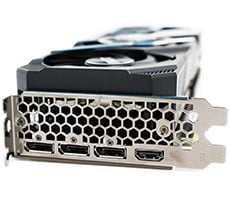
The outputs on the Radeon HD 5570 consist of a dual-link DVI output, a DisplayPort output, and a standard VGA output. Any combination of these ports can be used simultaneously. The card also fully supports 'ATI Eyefinity multi-display technology, with up to three displays.
The backside of the Radeon HD 5570 is exposed, but other than the myriad of surface mounted jellybean components, and a few memory chips there isn't much to see. The GPU heatsink retention bracket is visible right about in the center the PCB, but where the card's CrossFire edge connectors are supposed to be there are none. It is up to board partners though, whether or not to outfit their cards with CF connectors, but we doubt that will happen given the card's price point. Please note, that CrossFire is still supported with two of the cards pictured here; transactions will be sent over the PCIe interface, however, instead of the CrossFire bridge.


