Intel Patent Details Unique Adamantine L4 Cache For Next Gen Meteor Lake CPUs

This information comes from a patent that was actually filed way back in December of 2020. The patent isn't specifically about the Adamantine L4 cache itself, but references it in a note about "Next-generation client SoC architectures." The topic of the patent is actually "Early Platform Hardening Technology For Slimmer And Faster Boot," and it's mostly about how boot processes can be both more secure and speedier through using CPU SRAM for security processor operations instead of waiting for the initialization of system DRAM, or main memory.
Interestingly, the note accompanying the graphic goes on to say that "large on-package caches" will enable "novel usages" of said next-gen CPUs. Those apparently include "modern device use cases" such as "automotive in-vehicle infotainment" as well as "household and industrial robots, etc." It closes with the optimistic statement, "accordingly, new market segments may be available."

Image: Intel Patent
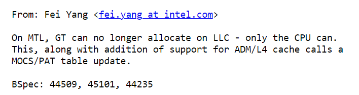
Analysis of the block diagram graphic itself is quite fascinating. All of the processor tiles rest on the "ADM base or passive interposer," implying that Meteor Lake processors could be created without the Adamantine L4 cache. The block diagram clearly illustrates four tiles on top of the base tile, just as we've seen in Intel's other documents. Those are the GPU tile, the compute tile, the SoC tile, and a fourth tile labeled here as "PMC," likely "Power Management Controller."
In this specific processor the GPU is based on "Gen 12.7" architecture, better known as Alchemist. It's specifically labeled as having 64 EUs, which would give it 512 shaders. That's a fairly potent GPU for a processor that has just two Redwood Cove P-cores and eight Crestmont e-cores, although another fascinating point on the slide is that there appear to be two more Crestmont cores on the SoC tile.

Image: Igor's Lab
We reckon that these two extra cores are likely the "LP E-cores" mentioned in this slide leaked last year by Igor's Lab. Other curious details in the diagram include the presence of a GNA neural accelerator, and the placement of the media engine, display engine, and four display pipes on the SoC tile instead of on the graphics tile.
Intel has Meteor Lake slated for release in the second half of this year, and rumors say that the first released processors will be mobile chips. Stay tuned for more information as soon as we get it.
