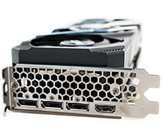
NVIDIA nForce 790i SLI Ultra and GeForce 9800 GX2
Below we have a high-level overview of the nForce 790i SLI Ultra chipset's high level architecture and main features. As the illustration shows, the 790i SLI Ultra (and non-Ultra version of the chipset) is a two chip solution consisting of the nForce 790i Ultra SLI SPP in the traditional Northbridge position and the 790i SLI Ultra MCP in the Southbridge position.

NVIDIA nForce 790i SLI Ultra Chipset Diagram
The chipset has full support for all Intel desktop processors with front side bus speeds as high as 1600MHz. The DDR3 memory controller in the SPP is compatible with EPP 2.0 and officially capable of speeds up to 2000MHz, although higher speeds are possible with overclocking. 32 of the chipset's PCI Express lanes reside in the SPP, with the remainder coming by way of the MCP. And the two chips are linked via HyperTransport. We should note that the SPP's lanes are gen 2, while the rest are gen 1. What NVIDIA has done here is essentially bring the NF200 chip present on the 780i SLI and 750i SLI chipsets and brought it right onto the SPP.
Although the nForce 790i Ultra SLI MCP has a new name here in the block diagram, it is still the NF570 chip used on motherboards dating back to the introduction of the nForce 500 series. It would be nice if NVIDIA revamped this chip and produced it on a more advanced process node to bring power consumption down, but from a feature standpoint it's still as robust as any other solution currently on the market.

NVIDIA nForce 750i SLI Chipset Diagram
The nForce 750i SLI's feature set is similar to its high-end counterpart in some respects. Both chipsets support all current Intel processors and both are linked via HyperTransport. The nForce 750i SLI, however, utilizes a third chip - the NF200 - for its PCI Express 2.0 connectivity and the chipset has fewer PCI Express lanes overall. The nForce 750i SLI's MCP is also pared down a bit with fewer USB and SATA ports, and only a single Gigabit Ethernet controller.


