Intel Xeon Scalable Debuts: Dual Xeon Platinum 8176 With 112 Threads Tested
Despite the SP designation, at its core, the architecture is similar to the original Skylake that previously appeared in Intel’s mainstream CPU line-up. As such, we won't be going too in-depth again here. For deeper coverage of Skylake, we strongly suggest checking out our launch piece. Skylake-SP, however, has received some significant updates worth mentioning.
Before we dive into the big changes, here’s a quick-take on what Skylake brings to the table versus the previous-gen Broadwell and Haswell micro-architectures. Skylake has gotten “wider and deeper”, in that it can handle more in-flight loads and stores, and scheduler entries. It also has larger register files and allocation queues as well. The branch predictor and prefetcher have been updated too and it has an improved divider. Ultimately, the changes in Skylake help improve IPC and efficiency while introducing more instruction-level parallelism, to improve performance across an array of workloads.
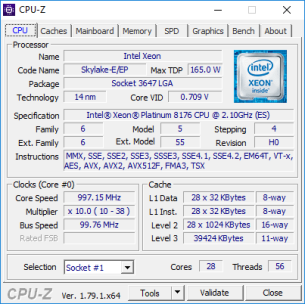
Intel has also completely restructured the cache hierarchy in Skylake-SP. The design quadruples the size of the L2 cache, bringing it up to 1MB per core, but reduces the size of the shared L3. In its entirety, however, there is still roughly the same amount of total cache. Not only have the cache sizes changed, but how they are utilized has been changed as well.
With previous-gen processors, an inclusive cache structure was used. With such a large L2 cache, however, an inclusive cache didn’t make sense anymore, because entire copies of the cache data needed to be maintained in both places, which would effectively reduce the amount of L3 available. And duplicating such a large amount of L2 on a smaller L3, didn’t make any sense whatsoever. To increase the size of the L2 and keep the L3 cache size larger, Intel would have had to sacrifice core count to keep die sizes in check, so the decision was made to move to a non-inclusive cache structure. This change results in a better hit-rate in the larger, lower-latency L2 cache, and a negligible though somewhat lower hit-rate on the smaller L3. As you'll see in the benchmarks a little later, the Xeon Platinum 8176's performance scales as you would expect, so restructuring the cache doesn't seem to have completely changed the performance profile.
The better efficiency of Skylake-SP over previous generation Xeons has allowed Intel to push core counts and frequencies higher. Virtually all of the Xeon Scalable Processor family supports Turbo boost frequencies of various degrees to increase overall performance, at frequencies higher than the previous generation. Skylake-SP also features support for AVX-512 extensions, which are a set of new instructions that can accelerate performance for workloads like scientific simulations, financial analytics, artificial intelligence (AI)/deep learning, 3D modeling and analysis, image and audio/video processing, cryptography, and data compression.
AVX-512 code can feature eight double precision (DP) and sixteen single precision (SP) floating point numbers within the 512-bit vectors, as well as eight 64-bit and sixteen 32-bit integers. This enables worker threads to achieve more work per CPU cycle (with double the width of data registers) and helps to minimize latency and overhead (with double the number of registers), compared to AVX2. Applications must be coded to support AVX-512, however, and when AVX-512 is used the processors will scale to lower frequencies, then non-AVX workloads. The actual AVX-512 frequencies will vary from processor to processor, but are generally a few speed-bins below the typical Turbo boost frequencies.
Versus previous-gen processors, Skylake-SP can also switch P states (power states) much faster. Skylake-SP can control P states fully in hardware in as fast as 1ms, whereas older processors required OS control. It takes roughly 30ms to switch with older processors and architectures. Though it doesn’t affect peak performance of the processor, hardware controlled P states can enhance responsiveness and efficiency, because the processor is able to ramp up and down more quickly.
Linking all of the cores, cache, and I/O in Skylake-SP is a new mesh architecture. In previous-generation, many-core Xeon processors, Intel employed a ring interconnect architecture to link the CPU cores, cache, memory, and various I/O controllers on the chips. As the number of cores in the processors, and memory and I/O bandwidth has increased, however, it has become increasingly more difficult to achieve peak efficiency with a ring interconnect, because it could require data to be sent across long stretches (relatively speaking) of the ring to reach its intended destination. The new mesh architecture addresses this limitation by interconnecting on-chip elements in a more pervasive way, to ultimately increase the number of pathways and improve efficiency.

In addition to the new mesh, a new link dubbed UPI is being used to link the processors to each other in multi-CPU setups and to the PCH. UPI, or the Ultra Path Interconnect, supersedes QPI and offers higher-speed links with more bandwidth to improve messaging efficiency. Higher-end Xeon Scalable Processors feature up to three UPI links to better accommodate the additional memory bandwidth afforded by the increased number of memory channels, and enhance performance with workloads that are not NUMA-optimized (Non-Uniform Memory Access). Intel could have cranked up the clocks on the older QPI links to achieve similar performance, but that would have come at the cost of power, hence UPI was created.


