Intel Core i7-3770K Ivy Bridge Processor Review
As we’ve already mentioned, Ivy Bridge is a “Tick” in Intel’s processor release cadence, so it is not based on a new microarchitecture, but rather the Sandy Bridge microarchitecture that came before it. While the processor cores themselves remain largely unchanged from Sandy Bridge, Ivy Bridge is built using a more advanced 22nm manufacturing process. Of course, Intel also uses the transition to a new process to introduce a few new features or tweak other parts of the chip as well.
;)
Intel Ivy Bridge Die Map
What you see pictured above is a die map of a quad-core Ivy Bridge processor with integrated Intel HD 4000 series graphics. The layout and general configuration looks much like Sandy Bridge, as you would expect, but there are some differences we’ll talk about in a bit.
Ivy Bridge consists of roughly 1.4 billion transistors and has a die size of approximately 160mm2. The on-die processor graphics and shared L3 (or LLC) cache dominate the die, with the CPU cores, memory controller and system agent (which includes DMI, display outputs, etc.) making up the rest.
Core i7-based Ivy Bridge processors will have 8MB of L3 cache, Core i5 processors 6MB, and Core i3s 3MB. Core i7 processors will also have the most powerful Intel HD 4000 series graphics engine enabled, while Core i5 and i3 processors will have either Intel HD 4000 or less powerful HD 2500 series graphics, depending on the model. Like previous generation Sandy Bridge-based processors, Core i7, i5, and i3 processors will also differ in their support for HyperThreading and whether or not they support performance tuning and are unlocked or partially unlocked via support for Turbo.
;)
;)
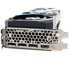
Intel Core i7-3770K Top and Bottom
With Ivy Bridge, Intel continues to use the same chip and platform configuration, and core microarchitecture as Sandy Bridge. Ivy Bridge has similar CPU cores, with on-die processor graphics. It also has a similar cache structure with shared LLC (Last Level Cache) and a modular on-die Ring Interconnect for high-speed, on-chip communications between the processor elements. Ivy Bridge has a similar dual-channel memory controller configuration and on-die PCI Express 3.0 connectivity as well. Ivy Bridge is also compatible with the same Socket 1155 as Sandy Bridge, although not every previous-gen Socket 1155 motherboard will support Ivy Bridge. We should point out, however, that the processor cores, LLC, and memory controller have all been optimized to offer improved performance in terms of IPC. There have also been enhancements made to the ISA for SSE.

32nm Planar Transistor (left) 22nm 3D Tri-Gate Transistor (right), Similar Magnification
Much has been borrowed from Sandy Bridge, but there are plenty of new things coming with Ivy Bridge too. As we’ve mentioned, the chips are the first to be built using Intel’s 22nm process node, which features Tri-Gate transistor technology. The smaller geometry in addition to the use of Tri-Gate transistors not only results in a smaller die, transistor for transistor, but better power characteristics as well. We’ve got more detail on Intel’s 22nm process and Tri-Gate transistor technology here for those that would like more detail.


Along with using a new process to build the chips, Ivy Bridge is outfitted with a more powerful graphics core with improved Quick Sync engine, improved overclocking capabilities, and support for three independent displays (up from two). In its full configuration, the new Intel HD graphics core in Ivy Bridge features 16 execution units—up from 12 in Sandy Bridge—with support for DirectX 11 and all that that entails, including hardware accelerated tessellation and support for compressed texture formats. The Quick Sync engine has also been beefed up with additional resources to offer even faster media encoding than Sandy Bridge.
There are some new security and power management related features incorporated into Ivy Bridge as well. On the security front, Ivy Bridge now has a built-in random number generator (which is designed to be standards compliant) and supervisory-mode execution protection. SMEP is designed to help prevent Escalation of Privilege attacks, by preventing execution out of untrusted application memory, while operating at a more privileged level. In regard to its new power management features, Ivy Bridge now has a configurable TDP and new low-power mode to enhance battery life on mobile platforms. DDR I/O now has embedded power gating and low-level design optimizations have resulted in lower S3 power consumption. Ivy Bridge also has Power Aware Interrupt Routing (PAIR), which chooses the best core to service interrupts based on the current optimization mode (power vs. performance).