Intel Core i7-2600K and i5-2500K Processors Debut
As we’ve mentioned, the Sandy Bridge microarchitecture is almost completely new. The out of order execution engines and the Floating Point units in Sandy Bridge were re-designed from the ground up in an effort to further optimize for power efficiency and performance over previous Intel processor designs. In the OOO engines, Intel went to a physical register file. This reduces die area and can also lower power because it eliminates duplicated data in various registers and minimizes the amount of of data movement around the chip. This, and other techniques used in the OOO engines allowed Intel to incorporate larger OOO buffers, which also provide a bigger window to find Instruction Level Parallelism (ILP), which can increase performance on legacy code. The reduction in register space and data movement is also essential for AVX (Advanced Vector Extensions), where data vectors are 2x the size of previous generations. AVX is a new set of instructions in Sandy Bridge that improves Floating Point and Vector computation performance. Sandy Bridge is also outfitted with new micro-op cache. The decoded micro-OP cache provides high and consistent bandwidth, at much lower latency, than the traditional front end decode path. It also provides the UOPs at much lower power than the traditional front end.

The brand prediction units in Sandy Bridge were also completely redesigned. Intel’s branch predictors in Nehalem were already very efficient, but changes were made to the branch predictors in Sandy Bridge to provide more accuracy through more branch targets, more branch history and other mechanisms, while keeping similar die area to Nehalem. According to Intel, the changed here included “better representation of the additional information (such as longer history) in the same or similar amounts of bits. For example, split targets into close ones (that require less address bits for knowing the distance) and far ones (that require all the address bits). Similarly for history – find out what history can be reduced, and use the freed-up bits for the branches that require more history.”
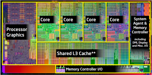
The cache structure in SB is somewhat of a departure from previous designs as well. There are specific amounts of L1 and L2 cache per CPU core and a larger Last Level Cache that both the CPU and graphics cores can share. The LLC helps both 3D graphics and Media (video) by providing very high bandwidth, low latency and low power data repository. Intel also built in a fine grained shared cache control at the per data stream (or data buffer) level for the graphics core that allows us to fine tune the cache sharing. For example, for H.264 video decoding, Intel was able to cut down the DRAM bandwidth by roughly 50% by mapping small scratch buffers to the last level cache while allowing other large video buffers to bypass the LLC.
Another new feature of Sandy Bridge is a high-bandwidth, low-latency ring bus that links all of the core elements in the processor. The system agent, CPU execution cores, graphics core, and last level cache are all linked on the ring bus, which is used to quickly route date to and from these core processor elements.
Making a return on Sandy Bridge is Intel’s Turbo Boost technology, but it too has been revamped. In addition to allowing the CPU cores to be dynamically overclocked, Turbo can also boost the frequency of Sandy Bridge’s integrated graphics core as well. In addition, the new Turbo Boost implementation will also allow Sandy Bridge processors to run beyond their rated TDP in short spurts to further increase performance.


