AMD Zen 2 Architecture Explored: What Makes Ryzen 3000 So Powerful
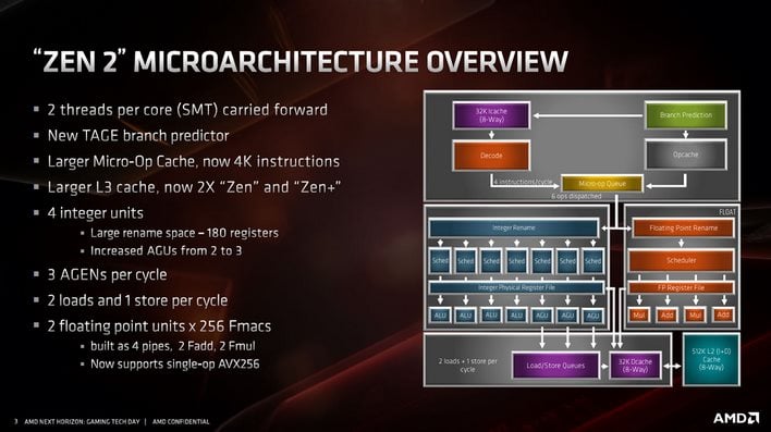
The amount of total cache in Zen 2 has been significantly increased as well. The L3 cache size has been doubled, up to 32MB. The larger L3 cache reduces effective memory latency, by reducing the number of calls out to main system memory. The larger L3 cache has such an impact on performance that AMD is actually branding it "AMD Gamecache."
The way the chips are packaged is changing with AMD's Ryzen 3000 series as well. With the Ryzen 3000 series processors, AMD is moving their mainstream CPU line-up to a multi-chip architecture approach, similar to what the company did with EPYC and Threadripper. The processors consist of mutli-core CPU chiplets (up to 8-cores / 16-threads per chiplet) that are linked to an I/O die, which then branches out to the main memory and the PCH (Platform Controller Hub). The CPU core chipsets are manufactured using a 7nm process and the I/O die, which also features a completely redesigned memory controller, is manufactured at 12nm, and AMD’s 2nd Generation Infinity Fabric ties everything together. The new memory controller has actually been able to hit 5,100MHz with air cooling (on upcoming X570 motherboards with optimized trace routing), but AMD is officially supporting up to DDR4-3200 speeds, which helps provide an overall performance uplift as well.
We should note that there are additional memory and Inifinity Fabric multipliers available for tweaking memory performance on Ryzen 3000 series processors. A 1:1 mode is available up to 3733MHz, which switched to a 2:1 mode at higher clocks. That 2:1 ratio, however, will negatively impact latency. The best latency will be at 3733MHz, but the higher bandwidth available with higher clocks will help with some workloads as well of course.
To cram the chiplets into the same size package / AM4 socket, AMD moved from traditional solder bumps to copper pillars with the 7nm compute dies. The I/O die, however, still uses solder bumps. The copper pillars are narrower and allow for higher density. And the pillars allow for uniform height as well. So with these microarchitecture, memory subsystem and packaging improvements, what can we expect in terms of specific Ryzen 3000 / Zen 2 performance? Let's look at that next...


