AMD Radeon VII Review: Performance Benchmarks With 7nm Vega
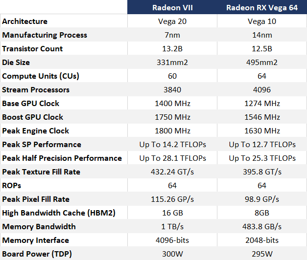
There is a lot to talk about with respect to the new Radeon VII. Below is a quick side-by-side of some of the Radeon VII’s main speeds and feeds versus the Radeon RX Vega 64. Take a quick look at the comparison to set expectations and then we’ll dive in a little deeper and see how the Radeon VII performs with a variety of games and workloads...
|
The move to 7nm allowed AMD to shrink the Vega 20 GPU die from 495mm2 on Vega 64 down to 331mm2 on the Radeon VII. According to AMD, this shrink and the subsequent silicon die area saving is what allowed them to add an additional two stacks of HBM2 memory and increase the high-bandwidth cache (frame buffer) capacity to 16GB on the Radeon VII -- Radeon RX Vega 64 cards have only 8GB of memory.
Roughly 700M transistors separate the two GPU designs, though in terms of their actual configuration, they are quite similar. The Radeon VII has 60CUs and a total of 3,840 active stream processors, versus 64CUs and 4,096 stream processors in Vega 64, but keep in mind that the full configuration of Vega 20 has the same CU and stream processor count. The Radeon Instinct MI60 has the full 64CU and 4,096 stream processor Vega 20 configuration, along with double the HBM2 memory. That’s interesting to note because it technically opens the door for a faster, fully-enabled Radeon VII variant at some point down the line, but we digress.
Although both cards use HBM2 memory, the Radeon VII’s is attached via a wider interface and is clocked slightly higher. The Radeon VII has a 4,096-bit wide memory interface – double that of Vega 64 -- with memory clocked at 1GHz (2GHz effective). With an interface that wide and at those clocks, the Radeon VII offers up a whopping 1TB/s (yes, Terabyte) of peak memory bandwidth, which is more than double that of its predecessor.
Radeon VII - Of Single And Double-Precision Compute Performance
Compute performance and fillrate are also increased on the Radeon VII versus Radeon RX Vega 64. There are the same number of ROPs on the Radeon VII, so its fillrate advantage comes by way of its increased clocks. The Radeon VII’s theoretical peak half and single-precision compute performance advantages are also the result of the GPU’s higher clocks, but we should note that some enhancements have been made in this regard as well. The Vega 20 GPU features additional floating point and integer accumulators versus the original Vega design, which can increase utilization, efficiency, and ultimately performance with some compute workloads. AMD had also previously communicated that Radeon VII would offer up to 0.88 TFLOPS (DP=1/16 SP) of double precision compute performance. However, based on customer interest and feedback the company decided to increase double precision compute performance to 3.52 TFLOPS (DP=1/4SP). As you'll see a little later, this has a big impact in performance in some workloads.All told, the Radeon VII should offer better performance than the Radeon RX Vega 64 across the board. In fact, AMD claims the Radeon VII is in the same performance class as the GeForce RTX 2080. AMD's new Radeon VII has more frame buffer memory, offers significantly more memory bandwidth, and peak compute performance and fillrate have been increased versus the Vega 64 as well. With all of that, the max board power has increased by a few watts – up to 300W on the Radeon VII – but in practice we found that the card actually consumed less power than the Radeon RX Vega 64.
The Radeon VII’s physical attributes are understated but attractive in our opinion. The design is clearly more minimalist versus NVIDIA’s latest GeForce GTX and RTX cards, but the Radeon VII looks good nonetheless. A brushed aluminum shroud with chamfered edges encases the front of the Radeon VII, with three axial fans evenly spread out across the front. At the upper-corner of the card, a lighted ‘R’ cube is present too.
The back side of the card also features a brushed aluminum plate, but with linear vents cut into it to add some visual flair. The GPU’s heatsink retention bracket is also exposed on the back of the card, along with a handful of screws that hold everything together.
Underneath the Radeon VII’s shroud is a large heatsink that covers the entire front of the PCB. The heatsink has a relatively thick copper base and vapor chamber that sits directly atop the GPU, with an array of flat, copper heat pipes running from the base out into the dense thin-fin heatsink array. There are vents on every edge of the card that allow air from the axial fans to escape from the card, save for the rear edge, opposite the case bracket which is completely sealed. We should also note that the RADEON logo on the top edge of the card is lighted, just like the little ‘R’ cube.
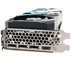
Two 8-pin PCI Express power connectors are present on the Radeon VII and its outputs consist of a trio of full-sized DisplayPorts and a single HDMI port. And all four of the outputs can be used simultaneously.
The first batch of Radeon VII cards to hit the market will all have a similar design to the one you see pictured here, but in time we suspect AMD’s board partners will offer up some custom solutions as well.


