Will Radeon GPUs Based On RDNA 5 Use Chiplets? Here's What We Know

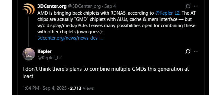
Despite what we've just said, though, it doesn't seem like AMD is planning to use GPU chiplets in quite the same was as it did with the Radeon RX 7000 series, and it also doesn't appear that AMD is planning to use multiple graphics chiplets on a single product—at least, not yet. That possibility was floated by our longtime comrades over at German hardware site 3DCenter, who posited the idea of AMD stacking multiple "GMDs" on a single GPU board, like so:
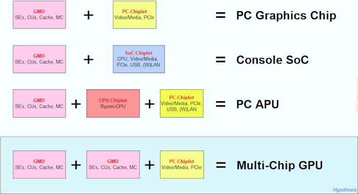
So what is a "GMD"? It is said to stand for "Graphics Memory Die," and is further said to be a chiplet that includes the core components of a graphics processor. That means shader engines, raster backends, and a memory controller, among other bits. What it supposedly doesn't include are a media block for video codecs, display output links, and a host bus interface, such as PCI Express. Those functions have to be supplied by a separate Media Interface Die (MID) chiplet, to which the GMD is hypothetically connected using TSMC's Local Silicon Interconnect—a high-speed silicon-based chiplet interconnect similar to Intel's EMIB.
Why separate those functions? So that there's less wasted silicon when a "GMD" is connected to another component. This can be an MID to form a discrete GPU, or an I/O chiplet that includes CPU cores, as is supposedly happening with the "Medusa Halo" products that will succeed the extant Ryzen AI Max "Strix Halo" processors. It can also apparently be a larger chiplet with CPU cores and other functions intended for a game console, as supposedly at least one of the upcoming next-gen game consoles will make use of an off-the-shelf RDNA 5 GMD for graphics duties.
Most of this information originates with the YouTube leaker Moore's Law is Dead, and we've already reported extensively on his claims. To briefly sum up, AMD is purportedly preparing no less than four new graphics dice, two of which will be more traditional GPUs that use GDDR6 or GDDR7 memory, and two of which will be these GMD devices that instead rely on LPDDR5X or LPDDR6 memory. This makes them better suited for use in APU designs that might suffer a performance penalty due to the use of high-latency, high-throughput GDDR memory, and it also makes them uniquely suited to lower-cost products thanks to the ubiquity of conventional LPDDR DRAM.
These GPU dice are apparently named after Transformers, with the GPU family being known as "Alpha Trion" (after the oldest living Transformer), while the chips for the PlayStation 6 and next-gen Xbox are known as "Orion" and "Magnus", respectively. AT0, the largest of the Alpha Trion GPUs, is so large that it may not actually come to consumer products, with compute throughput supposedly more than three times higher than the Navi 48 GPU used in the Radeon RX 9070 XT. The two smaller GPUs that are supposedly being used alongside CPU chiplets to form powerful APUs are AT3 and AT4.
It's an interesting inversion of the company's strategy with the Radeon RX 7900 series. Where those cards split the shader engines, memory interface, host bus interface, and media engines from the memory controller and cache, AMD is apparently doing the opposite. It makes sense in the context of what the company is purportedly planning with extreme chiplet re-use across product families. Hopefully we see a more concrete leak soon that proves or disproves these claims, because we're skeptical but seriously interested in this product line.
