Alleged AMD RDNA 5 GPU Diagrams Hint At A Massive 96 Compute Unit Flagship

We're going to use that as a bit of a launching off point to talk about the rumors regarding AMD's "RDNA 5" or, more likely, "UDNA" graphics cards. This architecture will form the basis of the company's next discrete GPUs as well as, supposedly, the next-generation home game consoles from Sony and Microsoft. If the rumors are correct, AMD is doing some pretty wacky stuff with the Alpha Trion series.

So looking at Kepler's diagrams of the two faster GPUs, AT0 and AT2, we can see that AT2 is already a large GPU, with forty UDNA compute units and a 192-bit memory bus. 40 CUs may not sound that big, but the current understanding is that UDNA will double the width of the compute unit. So saying, one UDNA compute unit is purportedly similar in capability to one RDNA 4 WGP, or "dual compute unit."
If that's the case, then AT0 looks absolutely massive. Sixteen 32-bit memory controllers yield a 512-bit memory interface, and 96 UDNA compute units is apparently similar to to 96 RDNA 4 WGPs, which is 192 RDNA 4 compute units. To put that in perspective, the powerful Radeon RX 9070 XT "only" has 64 compute units.
Both of these GPUs are expected to use fast GDDR memory, likely GDDR7, in combination with extremely expanded local caches. Rather than relying on a large "MALL" or chip-level cache as AMD did with RDNA 2 and RDNA 3—a simple but inelegant and expensive solution—AMD is apparently radically redesigning its chips at a lower level, allowing scheduling to happen at the Shader Engine level. This means that larger local caches, like the L0, L1 and L2, are more useful than a massive "Infinity Cache"—and cheaper in terms of die area, too.
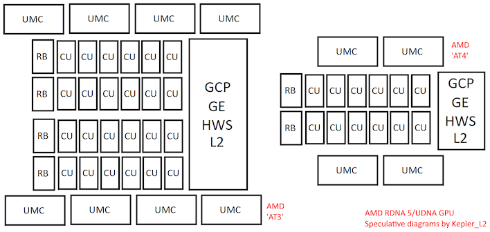
Meanwhile, the two smaller chips, supposedly known as AT3 and AT4, are arguably more interesting. AT3 is naturally the larger of the two, and what you might notice is that it appears to have a wider, 256-bit memory bus compared to the considerably more powerful AT2 above. The reason, if we believe Moore's Law is Dead, is because this chip is not in fact a typical discrete GPU, but rather a "GMD", or Graphics Memory Die. It hosts the GPU, as well as the memory interface, and can be used as the memory controller and "integrated" GPU along with a Ryzen SoC die.
As a result, these GPUs supposedly use LPDDR5X or LPDDR6 memory, since GDDR's long latencies would kill single-threaded responsiveness when used as system RAM. This development, in turn, means that AT3 and AT4 can come equipped with absolutely absurd amounts of RAM, because LPDDR5X and LPDDR6 come in denser packages and cost less than the pricey GDDR6/GDDR7.
It will be fascinating to see how discrete GPUs with LPDDR5X or LPDDR6 memory perform. We suspect that the memory bandwidth bottleneck is actually overstated and that performance will be better than most expect. We've done a lot of testing lately on this topic and found that there's definitely a threshold where more memory bandwidth doesn't help. As long as these GPUs can meet that 'threshold', they're golden.
Of course, this is ultimately all speculation based on rumors and the Instinct MI400's specifications, so take it with a whole packet of salt. AMD has said very little about RDNA 5 or UDNA, and we don't even know if the chips are at tape-out phase yet. Hopefully AMD does deign to deliver some information about its next-generation GPUs soon, because these rumors are getting wild.
