How AMD Zen 6 CPUs May Use TSMC's 2nm & 3nm Nodes For A Performance Boost

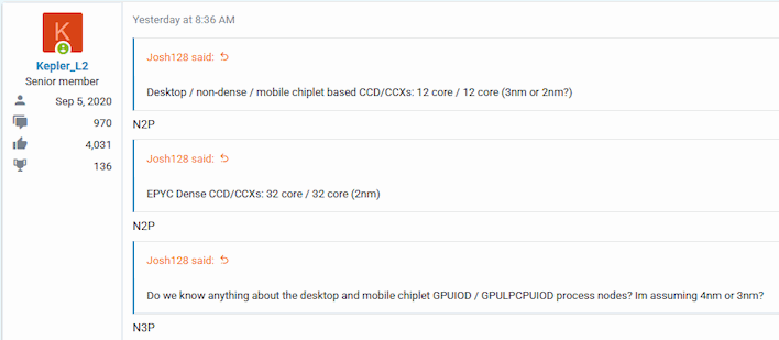
This information comes to us most recently from Kepler_L2, a noted leaker with a reasonably respectable history of accurate leaks. According to him, both the standard Zen 6 CCDs with twelve full-fat cores, as well as the dense CCDs used for high-core-count EPYC processors with a whopping 32 Zen 6C cores, will be manufactured on TSMC's N2P process, a refinement of N2 focused on high-performance, high-power designs.
This isn't the first time we've heard that, although the details differ slightly. Back in March, Moore's Law is Dead reported that the "Olympic Ridge" processors, the next-generation Ryzen desktop CPUs based on the Zen 6 architecture, will in fact use CCDs fabricated on TSMC's N2X process. N2X will be a later, further revision of N2P that targets even higher-power applications striving for the maximum performance. That kind of process technology will be required if AMD truly intends to reach 7 GHz with Zen 6 as Tom (MLiD) says.
Kepler also marks down the I/O die for TSMC's N3P. This fabrication process isn't as efficient as N2P or N2X, but the I/O dice don't use as much power as the compute tiles, and some components on them don't scale particularly well, meaning that the larger die becomes expensive to produce on smaller processes. Actually, MLiD claimed back in March that AMD might offer higher-end SKUs with an N3P cIOD while lower-end SKUs might get an I/O die built on TSMC N6, the very same used for the Ryzen 7000 and 9000 processors.

Interestingly, MLiD also claimed back in March that the processors with the N3P IOD would also enjoy an extra pair of Zen 5 LP CPU cores on said IOD. That would be a curious inclusion in a Zen 6 desktop processor, but assuming they support the same instruction sets it shouldn't cause any significant software issues. It's possible that the N3P IOD is meant for "Gator Range", the mobile version of "Olympic Ridge", to help with idle efficiency.
As far as the CCDs—the chiplets that contain the Zen 6 CPU cores—the distinction between N2P and N2X is meaningful. N2X is designed for high-voltage, high-performance designs that want the maximum possible performance, power draw be damned. It's entirely possible that we may see Zen 6 CCDs fabricated on both N2P and N2X, with some chips favoring N2P for higher efficiency while others use N2X for maximum clock rate—potentially that vaunted 7 GHz desktop SKU. However, chips built on N2X are likely to be considerably more expensive, too.
Whatever the case we just hope AMD announces something sooner than later. The company's plans for its Zen 6 processors, particularly its mobile "Medusa Point" and "Medusa Halo" families, sound too odd to be true, but we'd love to be wrong. Unfortunately, we probably won't know anything until next year at the earliest, because neither N2P nor N2X are slated for mass production until 2027, more than a year away.
