A series of Twitter posts are drawing attention because they purportedly detail
NVIDIA's next-generation
Ampere GPU, with some interesting (and potentially far-fetched) information. We're highly skeptical, for reasons we will discuss in a moment. However, it is fun to speculate as we await the next big GPU from NVIDIA, in what figures to be a busy year overall in the graphics space.
We already covered
what we know about Ampere to date, or think we know, based on past rumors and speculations. In short, past leaks indicate NVIDIA will be making a transition to a 7-nanometer manufacturing process, a place AMD is already at with its latest generation
Navi GPU architecture, and previous generation Vega. Ampere is also rumored to deliver a big performance uplift over
Turing, at half the power cost.
Will those things come to pass? It is impossible to know right now, though the previous claims are all the more interesting in light of newer rumors.
NVIDIA's Next Generation GA100 Ampere GPU Rumored To Be Massive
Let's get started with it, shall we? Twitter user KittyCorgi (@CorgiKitty) has drawn some attention over a handful of tweets regarding Ampere. The latest one, posted on Friday, claims Ampere will feature a die size of around 826mm
2. To put that into perspective, NVIDIA's current generation Turing GPU (12nm) tops out at 754mm
2 (TU012), with 18,600 million transistors, AMD's 7nm Navi GPU tops out at 251mm
2 (Navi 10), 14nm Vega (Vega 10) is 495mm
2, and 7nm
Vega (Vega 20) is around 331mm
2.
What makes KittyCorgi's claim interesting is not just the raw size, but the notion of NVIDIA unpacking a 7nm GPU that big. If Ampere does end up measuring 826mm
2, it seems more likely it would leverage a 12nm manufacturing process instead, which goes against previous rumors. But hey, anything is possible, right?
 Source: KittyCorgi (via Twitter)
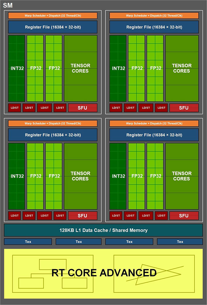
KittyCorgi also posted some diagrams they constructed based on the information they posted. Bear in mind that KittyCorgi is not claiming that these are leaked diagrams, hence why it is easy to spot details that are not consistent with real diagrams that NVIDIA produces.
That said, the supposed leaker makes the following claims about Ampere...
- INT32 Unit remains unchanged
- Double the FP32 Unit for shader proportion
- Double the Tensor Core performance
- Enhanced L1 data cache for more comprehensive functions
The diagram also points to a more advanced RT core design, which is an easy guess to make—RT cores are what power NVIDIA's real-time ray tracing efforts, and there is every reason to believe we will see both an increase in the number of RT cores and a tweaked design to allow for more performance, when Ampere arrives.
Source: KittyCorgi (via Twitter)
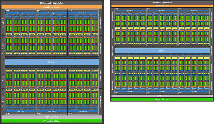
KittyCorgi posted a couple of block diagrams as well. The one on the left supposedly depicts a GA103 GPU and the one on the right highlights the GA104 GPU. As with the other diagram, these are not leaked slides, but ones KittyCorgi constructed based on the information they are leaking.
According to KittyCorgi, the higher end GA103 GPU will feature 60 streaming multiprocessors (SMs), 10GB or 20GB of memory, and a 320-bit memory bus. That would give the GPU 3,840 CUDA cores, which is less than the GeForce RTX 2080 Ti, though that's assuming NVIDIA sticks with 64 CUDA cores per SM. Being a much denser GPU, according to the information posted, we could be looking at 128 SMs per core, which would give the GA103 GPU 7,680 CUDA cores.
The GA104, meanwhile, is said to feature 48 SMs for either 3,072 CUDA cores (64 CUDA cores per SM) or 6,144 CUDA cores (128 CUDA cores per SM), 8GB or 16GB of memory, and a 256-bit memory bus.
Why The Latest Leaked Ampere GPU Specifications Are Definitely (Maybe?) Real
Nothing is official until NVIDIA says so, it is simple as that. But if you are looking for reasons why these specifications could be legitimate, it really boils down to Navi. How so? We know AMD is coming out with an upgraded version of Navi later this year, one that will bring performance to the fold, along with support for real-time ray tracing. A custom version of this so called '
Big Navi' will be featured in both Sony's
PlayStation 5 and Microsoft's
Xbox Series X game consoles, and AMD confirmed we will see Big Navi in the
PC space this year as well.
NVIDIA is not one to rest on its laurels. Big Navi could conceivably dethrone the
GeForce RTX 2080 Ti, which is something the
Radeon RX 5700 XT is not able to do. There is a perceived threat to the performance crown, and so Ampere is on tap.
Past rumors suggest Ampere will deliver big performance gains, both in rasterized rendering performance and ray-traced workloads. The supposedly leaked specifications would certainly keep NVIDIA in the lead, and probably by a big margin.
Why The Latest Leaked Ampere GPU Specifications Are Definitely Hogwash
While it is fun to consider a 7nm GPU with an 826mm
2 die size and 20GB of video memory piping data through a 320-bit bus, it all seems...optimistic. That's a tough ask of
TSMC (or any chip fab), and we see problems with yields at that density. All of the resulting defective dies means we would be looking at an astronomical price tag for working parts, and quite frankly, we don't see it happening. As in, go ahead and bet the farm against these leaked specs playing out.
If this does somehow come to pass, we are almost certainly looking at a server GPU, with consumer variants being less ambitious with better yields and better pricing. Still, our BS meter is ringing with this one. [EDIT: To be fair, KittyCorgi made the 826mm2 die size claim in regards to the GA100 GPU, which would be a server-bound chip rumored to have a 6,144-bit memory bus.]
There's also the source to consider. KittyCorgi has only been on Twitter for a month and has not built up a reputation as a leaker. So what this all boils down to is a fantastic claim by an unknown person with home-grown block diagrams.
We have little doubt Ampere will bring the boom, we just don't think the leaked specifications are going to play out.


