Intel Says Moore’s Law Is Alive And Well With Trillion Transistor Chips Coming By 2030
The biggest one is in the headline, of course: one trillion transistors on a package by the next decade. For perspective, the densest chip around is NVIDIA's AD102 used in the GeForce RTX 4090, and that's only got 76.3 billion. Hitting one trillion is going to require some enormous advancements in microprocessor fabrication. Regular readers may recall that Intel's CEO Pat Gelsinger committed to advancing five nodes by 2025, and gave the company's foundry division "unlimited" resources to accomplish that.
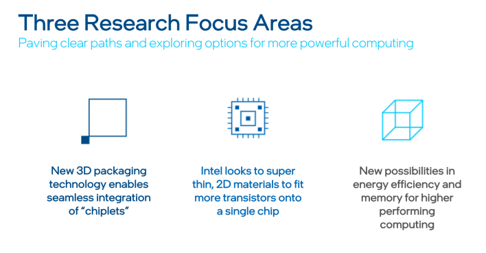
Well, judging by what Intel's brought to the IEDM show and tell, it looks like those efforts may be bearing fruit. The company is primarily presenting advancements in three key areas: 3D packaging technology, ultra-thin materials science advancements, and entirely new types of processors altogether.
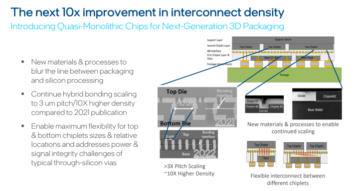
As it stands right now, chiplet-based (or "disaggregated") processors have two discrete stages: the chiplets are manufactured like any other microprocessor, and then those chiplets are carefully assembled into a complete package. Intel says it's looking to "blur the line" between these two stages, allowing greater connectivity between chiplets. AMD made similar remarks when talking about the fanout interface between chips on its Navi 31 GPUs.
Intel refers to chips fabricated with its next-generation technology as "quasi-monolithic," because the hybrid bonding in use, when scaled to 3μm interconnect pitch, apparently provides similar bandwidth to the same features found on monolithic SoCs. Despite that, the interconnects are apparently flexible in the sense that they can be used to connect to different chiplets, allowing versatility in product design.
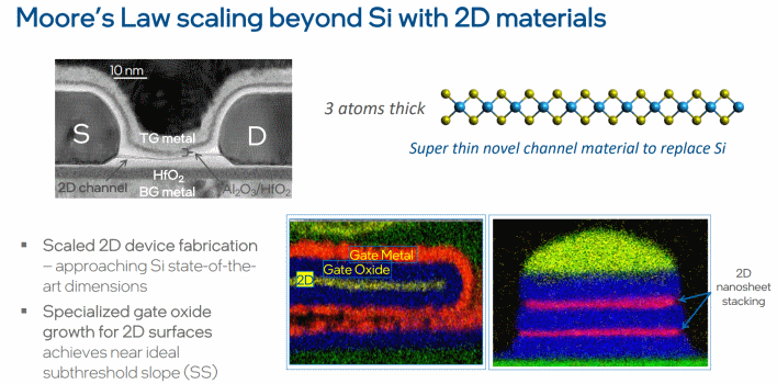
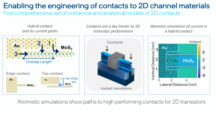
The main reason that progress on Moore's Law has slowed down in the last decade is because we're approaching the physical limits of traditional silicon fabrication. Intel looks to move beyond those limits by using new materials, including hafnia and molybdenum disulphide. These materials are known as "2D materials" because they are relatively easy to form into the complex structures needed for microprocessors while remaining flat.
A lot of people have written reams about the use of graphene in transistors, but despite its many attractive properties, graphene lacks one critical feature: a natural bandgap. That means that, to make graphene transistors, you have to engineer a bandgap yourself, and that's problematic for all kinds of reasons. Instead, Intel is looking at stacking 2D nanosheets using less exotic materials that come with an intrinsic bandgap, allowing them to make said nanosheets just 3 atoms thick.
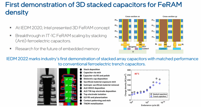
When you've got a problem to solve, you can try to improve the performance of your solution, or you can try a new solution. Intel's attacking both angles right now, and one of the examples of the latter idea is stacked FeRAM. Ferroelectric RAM is nothing new in its own right, but so far it hasn't seen much use because it suffers from extremely poor density compared to flash memory and DRAM.
Intel presented a concept for 3D-stacked FeRAM back in 2020, but since then, it's had a breakthrough in FeRAM scaling by stacking ferroelectric capacitors. According to Intel, this is the first demonstration of stacked array capacitors that can match performance to conventional trench capacitors. The company posits that this is very promising for the future of embedded memory, as FeRAM is fast, efficient, and non-volatile.
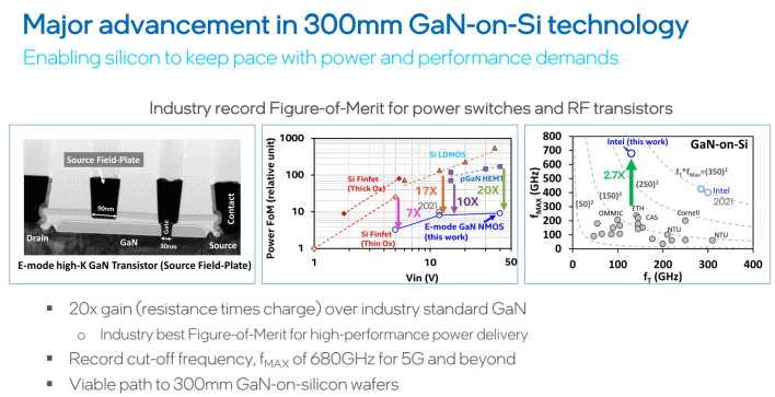
As transistor count rises, so too does the power consumption of the ever-denser chips. Intel's working on combating that too with its advancements in materials science. Gallium Nitride (GaN) semiconductors are popular in RF applications owing to their ability to handle considerably higher power and higher frequencies than traditional silicon chips.
Intel says its new GaN-on-Si technology offers a 20x improvement over the state-of-the-art in terms of power efficiency. What's more, the company has achieved a cut-off frequency of 680 GHz, which it says will enable development of ever-faster wireless tech beyond today's 5G. While GaN-on-Si is relatively expensive, Intel also claims that it has a "viable path" to doing it on 300mm wafers. That should reduce costs considerably.
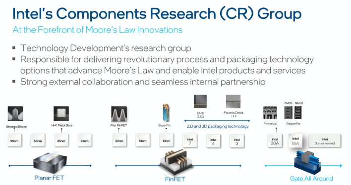
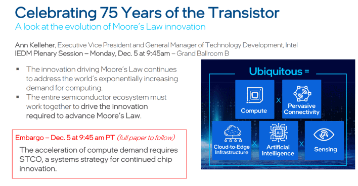
As the slide above says, Intel's celebrating 75 years of the transistor. Intel has undeniably been a driving force behind the creation of our modern world, and the company's research arm has been at the forefront of semiconductor technology for most of its history. In practical terms, Chipzilla may have fallen a bit behind TSMC, but it's clear that the folks in charge over there are well aware of the importance of bleeding-edge fabrication technologies.
The company's current products are fabricated on "Intel 7", but its 14th-generation Meteor Lake chips are supposed to hit tape out on Intel 4 any day now, which would put their launch early next year. After Intel 4, we've got a refinement called "Intel 3", and then a new process called "20A" still later. Intel says it will have the 20A refinement, known as 18A, ready before 2025. That'll be an impressive feat, but we're eager as anyone to see renewed competition in the foundry space.

