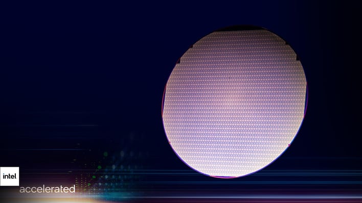
Intel Details Ambitious Chip Fab Roadmap With Cutting-Edge RibbonFET, PowerVia And Foveros Tech

Intel Renames Its Chip Fab Process Nodes
Before talking about the new transistor and packaging technologies, a discussion regarding Intel’s newly-disclosed node naming is in order. In years past, node naming typically coincided with a particular feature of the process technology, like the gate length or the half-pitch, which is half of the distance between two similar features in the silicon. Today though, a “smaller” node name does usually correlate to a more advanced process, but isn’t necessarily indicative of any one particular measurement. Muddying the waters further, different foundries don’t necessarily adhere to all of the same benchmarks, so making direct comparisons between seemingly similar nodes – even if they’re branded with identical nanometer monikers – isn’t ideal.The disparity in process node naming has been going on for a number of years. So, Intel decided that now is the time to change things up and reveal new naming for its process nodes.

The current 10nm SuperFin process keeps its name. But the technology previously referred to as Enhanced SuperFin, which will be used for Alder Lake and Sapphire Rapids, will be re-branded Intel 7. The future process we’ve been referring to as 7nm, which will be used on Meteor Lake and the Granite Rapids compute tile (among other devices), will be known as Intel 4. The next-gen process beyond 7nm / Intel 4 will be called Intel 3, and as we move into the angstrom era (an angstrom is equal to a unit length of one hundred-millionth of a centimeter), that future node will be branded Intel 20A. Presumably, the additional numbers and letter designation will give Intel some headroom for additional branding differentiation down the road.
Related to all of this news, Intel also disclosed that it plans to quickly adopt next-generation extreme ultraviolet lithography (EUV), referred to as High Numerical Aperture (High NA) EUV, and that the company is set to receive the first High NA EUV production tool in the industry.
Intel 20A’s PowerVia And RibbonFET - New Bleeding-Edge Chip Tech
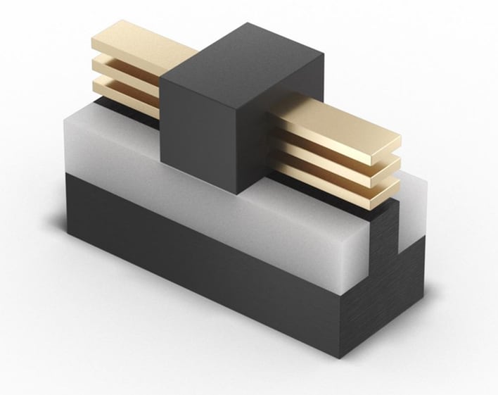
Intel has a long history of transistor innovations, from Strained Silicon, to Hi-K Metal Gates, FinFETs and the current 10nm SuperFin. Coming with Intel 20A are two innovations Intel is calling PowerVia and RibbonFET.
PowerVia is a power delivery system, where power will be fed into the chip from the back-side, while the front-side will be used primarily for data routing. PowerVia will optimize signal transmission by eliminating the need for power routing on the front side of the wafer. The end result according to Intel is higher density and a significant reduction in voltage droop.
As you can see in the images above, RibbonFET is essentially a nanoribbon that wraps completely around the channel. RibbonFET marks Intel's first new transistor architecture since the FinFET arrived in 2011. According to Intel, RibbonFETs will offer faster transistor switching speeds, at the same drive current as multiple fins, but in a smaller footprint.
Foveros Omni And Foveros Direct
Intel has a number of packaging innovations coming down the pipeline as well, which will fall under the Foveros umbrella. If you recall, Foveros refers to the 3D face-face die stacking packaging technology, which complements EMIB, or the Embedded Multi-Die Interconnect Bridge, used in processors like Kaby Lake-G.While on the subject of EMIB, Intel disclosed some updates to that technology as well. First off, upcoming Sapphire Rapids-based products will be the first family of Xeon processors to ship in volume with updated EMIB tech. That is the first dual-reticle-sized device in the industry, which Intel claims delivers nearly the same performance as a monolithic design. Beyond Sapphire Rapids, the next generation of EMIB will move from a 55-micron bump pitch to 45 microns, to further increase density.

Foveros Omni will leverage copper columns, to enable more flexible designs, by affording the ability to mix multiple top die tiles designs with multiple base tiles, across mixed process nodes. Foveros Omni also offers higher bandwidth interconnects, with optimized power and IO, and it reportedly minimizes any penalties associated with through-silicon vias as well.
Foveros Direct is a new, copper-to-copper bonding process that effectively enables an ultra low-resistance, direct copper connection between dies. With Foveros Direct, which offers a sub-10-micron bump pitch, bump density will see a massive increase to 10K per square millimeter. To contrast that increase, first-gen Foveros introduced at 10nm has a bump density 828/mm². Foveros Direct complements Foveros Omni and both are expected to be ready for volume manufacturing in 2023.
Gelsinger also boasted that the research and development for the manufacturing process innovations disclosed during the 'Intel Accelerated' webcast were primarily developed in the U.S., at Intel’s Oregon and Arizona facilities, and that they lay the foundation not only for future Intel products, but its partners as well. In fact, Intel's Foundry Services apparently has its first two customers. “The innovations unveiled today will not only enable Intel’s product roadmap; they will also be critical for our foundry customers,” Gelsinger said. “The interest in IFS has been strong and I’m thrilled that today we announced our first two major customers. IFS is off to the races!” Qualcomm is apparently on-board and has partnered with Intel to leverage the Intel 20A node.
The stream concluded with a confirmation that Intel's InnovatiON event will be held live in San Francisco and online October 27-28, 2021. You can bet we'll be at InnovatiON and that Intel will have a lot more to say then.
