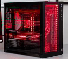
NVIDIA GeForce GTX Titan Powered Maingear SHIFT
The GK110 GPU powering the GeForce GTX Titan is technically not new. In fact, we first started talking about the GK110 in May of last year, when NVIDIA first revealed it at GTC 2012. You can read some of our initial coverage here and more here in a follow-up we posted a few months later when NVIDIA officially launched the Tesla K20 and K20X featuring the GK110.
;)
The GK110 GPU is massive to say the least.
To recap, the first thing you need to know about the GK110 is that the thing is a monster. The GK110 is comprised of roughly 7.1 billion transistors (yes, billion—with a B), which is over three times the number of transistors used in Intel’s Sandy Bridge-E based Core i7-3960X processor and twice as many as GK104 which powers the GTX 680. NVDIA has these chips built using TSMC’s 28nm process node.
;)
NVIDIA GK110 High-Level Block Diagram
The GK110’s original design features 15 SMX clusters, each with 192 single-precision CUDA cores and 64 double-precision cores, for a grand total of 2880 SP cores and 960 DP cores. Please note, however, that one SMX is disabled in every GK110 to keep yields acceptable, which brings the actual, workable core counts to 2688 (SP) and 896 (DP). As configured on the GeForce GTX Titan, the GK110 GPU also features 224 texture units, 48 ROPs, 1.5MB of L2 cache and a 384-bit memory interface, up from 256-bits on the GK104.
;)
A Close-Up of a single SMX in the GK110
At the 836MHz / 876MHz base and boost GPU frequencies defined by NVIDIA’s reference specifications, the GK110 can offer up to 4500 Gigaflops of compute performance and a textured fillrate of 187.5 GigaTexels/sec. On the GeForce GTX Titan, the GK110 is paired to a whopping 6GB of GDDR5 memory operating at an effective data rate of 6008MHz, for a peak 288.4 GB/s. If you’re keeping track, that’s about a 47% higher fillrate than the GeForce GTX 680 and nearly 100 GB/s of additional memory bandwidth.