NVIDIA GeForce GTX 570 DirectX 11 GPU Review
 Hot on the heels of the arrival of their flagship GeForce GTX 580, NVIDIA is launching another new graphics card based on the GF110 GPU. As we’ve come to expect from NVIDIA, and AMD for that matter, when a new GPU arrives, derivatives based on pared-down version of the chip typically get introduced, but with somewhat lower specifications. Such is the case with the GeForce GTX 570 we’ll be showing you here today.
It’s almost funny to say “somewhat lower specifications”, however, because the GeForce GTX 570 is one heck of a powerful graphics card, as you’ll see. We’ve got the full specifications outlined below, followed by a complete set of performance numbers using both a reference card and factory overclocked model from EVGA—the GeForce GTX 570 SuperClocked Edition.
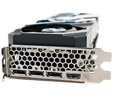
Unlike the GeForce GTX 470 which was based on a difference PCB than the GeForce GTX 480, and differed in a number of other ways as well, the new GeForce GTX 570 is almost indistinguishable from the GTX 580. There are differences in terms of its clocks, cooler, number of CUDA cores, and memory configuration, but without pulling the card apart you wouldn’t know it. The GeForce GTX 580 proved to offer awesome performance, and relatively quietly as well, so any similarities to the flagship are welcome ones in our book.
OK, time to dive in. Here are the GeForce GTX 570’s features and specifications (for the reference card). Pictures and more detail are on the next page, followed by the performance scores...

The NVIDIA GeForce GTX 570
|

Looking at the above features and specifications, it's obvious that the new GeForce GTX 570, like the GTX 580, is very similar to the GeForce GTX 480, which was released a few months back. In fact, the GF100 GPU (GTX 480) and GF110 (GTX 580/570) share the same architecture and feature set. As such, we'd strongly recommend checking out our coverage of the GeForce GTX 480 launch for the full scoop on what NVIDIA's high-end DirectX 11-class GPU can do, because we're not going to re-hash it all again here. With that said, the GF110 is a refinement of the GF100 design and some changes have been made to the ROPs and at the chip level.
Like the GF100, the GF110 is comprised of roughly 3 billion transistors and is manufactured using TSMC's 40nm process node. The GPU features 512 CUDA cores, 16 geometry units, 4 raster units, 64 texture units, 48 ROPs, and a 384-bit GDDR5 memory interface. “Only” 480 cores, 15 SMs, 60 texture units, and 40 ROPs are enabled on the GTX 570, however. No question, for a midrange card, the 570 has serious muscle.
The reference GPU clock is 732MHz, with 1464MHz shaders, and 1.28GB of 950MHz (3800MHz effective) memory. Please note, however, that the GTX 570 has a 320-bit memory bus, as opposed to the full 384-bits the GPU is capable of. The combination of 950MHz memory and a 320-bit memory bus results in 152GB/s of peak bandwidth, when clocked at reference specifications.