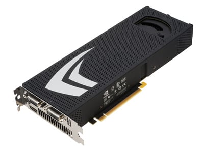
NVIDIA GeForce GTX 295 Unleashed
There's no doubt that the 3D Graphic Card business is what you'd call a proverbial "tough gig". There was a time when discreet graphics card options were available from numerous GPU vendors, but over the years, the relentless pace of technology and fierce competition has homogenized the market down to virtually two primary suppliers. In mainstream 3D Graphics, there is but one mantra--keep pace or exceed, execute or die. It's a simple equation that keeps product refreshes ongoing and a natural progression of the graphics food chain that results in continuously improved product offerings, at both the hardware and software levels.
NVIDIA is obviously one of the few companies, along with AMD's ATI graphics division, that has executed amazingly well over the years. The continuous strike / counter-strike battle that rages on between the two companies affords consumers increasingly more powerful products, as well as more realism in 3D games, as developers take advantage of each new technology update. In 2008, NVIDIA had the fastest single GPU solution on earth with the GeForce GTX 280, while AMD's ATI Radeon HD 4870 X2 took the most powerful single card performance spot with its dual, 55nm RV770 GPU solution.
Today, fresh out of the gate for 2009, NVIDIA returns AMD's volley with their own optimized, multi-GPU, single card solution that aims to trump their rivals once again. NVIDIA's GeForce GTX 295 is unleashed today. With a pair of 55nm GT200B GPUs under its hood in a pseudo-single card, dual slot height configuration, it's direct competition for the ATI Radeon HD 4870 X2. We'll step you through the technology behind NVIDIA's new single card SLI-enabled beast and then clock it around the benchmark track with some of the latest, most popular game titles on the market.
|
|
|
| GPU: Fabrication Process: 55nm Processor Cores: 480 ROP Units: 56 Texture Filtering Units: 160 Core Clock (MHz): 576 MHz Shader Clock (MHz): 1242 MHz Texture Filtering Rate: 92.2Giga Texels/s Memory: Memory Clock (MHz DDR): 1998 MHz Total Memory Config: 1792 MB Memory Interface Width: 448-bit per GPU Total Memory Bandwidth: 223.8GB/s Display Support: Maximum Digital Resolution: 2560x1600 Maximum VGA Resolution: 2048x1536 Standard Display Connectors: 2 x Dual-Link DVI-I, 1 x HDMI |
Feature Support: NVIDIA SLI-ready: Quad-SLI NVIDIA PureVideo Technology-HD NVIDIA PhysX-ready NVIDIA CUDA Technology HybridPower Technology GeForce Boost Microsoft DirectX 10 OpenGL 2.1 Bus Support: PCI-E 2.0 x16 Standard Graphics Card Dimensions: Height: 4.376 inches (111 mm) Length: 10.5 inches (267 mm) Width: Dual-slot Thermal and Power Specs: Maximum GPU Temperature (in C): 105 Maximum Graphics Card Power (W): 289 Power Connectors: 6-pin x1, 8-pin x1 |
Looking closely at the spec list above, you'll note that the GeForce GTX 295 looks like a double-shot of the GeForce GTX 280 on a single card but with GTX 260 core clock and memory speeds, as well as the GTX 260's slightly narrower memory interface. More details on this later, but beyond that we should also point out that the new GeForce GTX 295 also has a texture fillrate that comes close to a pair of GeForce GTX 280s in SLI.
In terms of the underlying technology behind NVIDIA's GT200 family of GPUs, as well as detailed explanations on many of their features, we'd suggest perusing one or more of the following HotHardware articles covering NVIDIA's previous GPU architectures:
- NVIDIA Geforce GTX 280 and GTX 260 Unleashed
- GeForce 8800 GTX and 8800 GTS Launch
- GeForce 8800 GT: G92 Takes Flight
- GeForce 8800 GTS 512MB Refresh
- GeForce 9800 GTX Launch
- GeForce 9800 GX2 and nForce 790i SLI Launch
Our GeForce 8800 GTX launch article goes in depth on NVIDIA's previous generation G80 GPU architecture and explains NVIDIA's CUDA GPGPU technology. Also, our GeForce GTX 280 and GTX 260 article covers much of the base NVIDIA GT200 GPU architecture, that is employed in 55nm technology now on the new GeForce GTX 295 we'll be covering for you in the pages ahead.


