AMD previously only teased bits of detail regarding their forthcoming 6th Generation A-Series APU, code named "Carrizo." We heard from AMD about this next generation, highly integrated mobile architecture as
far back as CES 2015 in January and then again
in February and more recently with AMD's HSA (Heterogenous System Architecture)
1.0 spec roll-out in March. It's safe to say AMD has been beating the drum on Carrizo with a regular cadence for the better part of 6 months now and today the company is finally going to full kimono on all details of their upcoming processor silicon and its platform.
Carrizo takes the fight to AMD's primary competitor in the lucrative premium notebook space, targeting a 15 Watt TDP (Thermal Design Power) envelope that sits square in the middle of Intel's ultrabook product stack. Think Core i5-5200U and up in Broadwell flavor (4200U in Haswell silicon) and that's the sweet spot of Carrizo. For AMD's purposes, of course, that's where the lion's share of the volume is in notebooks as well.

 AMD Carrizo: Integrated Southbridge, HSA, H.265 Hardware Assist and More
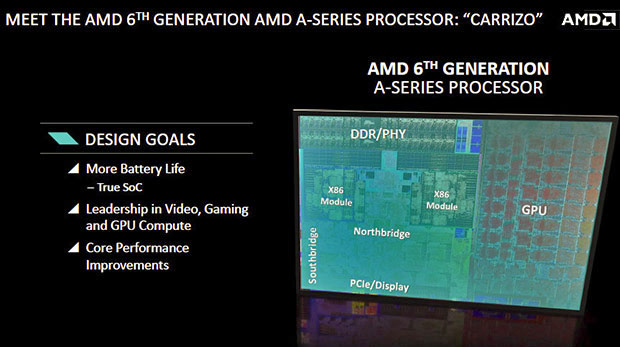
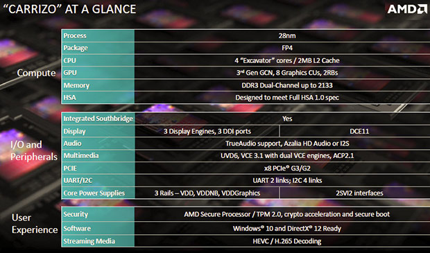
Carrizzo brings a number of firsts to the table for AMD and for the industry, actually. AMD's Carrizo APU is the first SoC architecture to fully support the HSA 1.0 specification, allowing full memory coherency and visibility of a shared memory space for both CPU and GPU. More on this shortly. Carrizo is also the first integrated APU to include full support in hardware for H.265/HEVC HD video decoding and finally, Carrizo is also the first AMD APU to have a full integrated, in silicon, Southbridge controller block, something Intel has yet to integrate. This isn't just a multi-chip module, on-package integration for Carrizo either, it's a full on-die integration with the rest of the SoC design. So, with its CPU, GPU, memory controller, Northbridge, Southbridge, and PCIe 3.0 links, Carrizo is truly a fully integrated System On A Chip.

One of the ways AMD was able to build these additional silicon resources into Carrizo was due to its more optimized "Excavator" CPU core architecture that affords the design a 23 percent silicon area reduction while still beefing-up resources in key areas. This was all achieved in the same 28nm manufacturing process as the previous generation Steamroller core, but with a higher density design library that allowed AMD to pack more features into less area. Let's dive a bit deeper into Carrizo's high level engine blocks, next...


