Intel Nova Lake Compute Tile Die Sizes Leak Highlighting Massive L3 Cache Expansion

Unlike AMD's solution and contrary to earlier rumors, it seems like Intel's bLLC may simply be part of the compute tile of the chip rather than stacked above or below it. We say that based on the latest leak from HXL (@9550pro on Xwitter), who claims that the Nova Lake compute tile is around 110mm² normally, or around 150mm² in its bLLC version. That's a huge jump in die area on an already large tile, and there's not a lot of other explanation besides that the increased L3 cache is included directly on the compute tile.
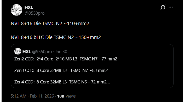
This is challenging for a few reasons. For one, as we noted, the Nova Lake compute tile is already rather large. Even frequent Intel leaker Jaykihn's earlier conservative estimate was large, at 96mm²; for comparison's sake, AMD's twelve-core Zen 6 CCD is said to be approximately 76mm², which is a touch larger than the Zen 4 and Zen 5 CCDs, with the slight change coming from the step change in process density (TSMC N2 uses nanosheets) and from the 50% increase in core count and cache size.
Some rumors have also posited that Zen 6 may increase the L2 cache of the CPU core all the way to 2MB, double what Zen 5 has. This ends up matching—sort of—the rumored configuration of Nova Lake, where each pair of P-cores shares a large 4MB L2 cache. The core counts are closer than you think, too; traditionally, four Intel E-cores was approximately the size (typically a bit larger) compared to a single P-core. with that in mind, eight P-cores plus four e-core clusters should be rather similar to twelve Zen 6 cores, at least in theory. In practice it sounds like Intel's chip is going to be considerably larger in the stock configuration.

Image: Intel
Die area is an interesting specification, because it's critically important to some parts of the product and completely irrelevant to others. End-users really don't have much reason to care about die area, for example. It does give us an interesting window into the design process and helps us speculate on things like pricing and availability. If the Nova Lake compute tiles are indeed as large as claimed, it's going to have to really be a performance monster to justify itself.
