NVIDIA GeForce GTX 560 Ti Review
The reason we bring up the GeForce 4 Ti is that NVIDIA is resurrecting the Ti moniker with a new GPU targeting mainstream market segments, dubbed the GeForce GTX 560 Ti. If you’ve been on top of the graphics space the last few months, you’ll no doubt be aware that NVIDIA recently introduced the GeForce GTX 580 and 570, which feature the GF110 GPU; an updated version of the GF100 which arrived with the GeForce GTX 480. In a similar move, the GF114 GPU that powers the new GeForce GTX 560 Ti is a new take on the GF104, which debuted on the GeForce GTX 460 a few months back.
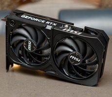
We’ve got a couple of GeForce GTX 560 Ti cards in the lab, a reference model from NVIDIA and a factory overclocked speedster from MSI. Strap yourself in and come along for the ride as we check out what will undoubtedly be a popular card with budget conscious PC gamers.

NVIDIA GeForce GTX 560 Ti Reference Card
|

![]()
The reference specifications for the new GeForce GTX 560 Ti are listed in the table above. While the numbers don't seem to align themselves with any previous GPU from NVIDIA, the GeForce GTX 560 Ti is actually very similar to the GeForce GTX 460. Let us explain.
The GF114 GPU at the heart of the GeForce GTX 560 Ti is actually an update to the GF104 used on the GTX 460. As was the case with the GF110 on the GeForce GTX 580, which was essentially a reworked GF100, the new GF114 is a respin of the GF104. In terms of features, the GF114 remains unchanged, but NVIDIA worked with their foundry partner, TSMC, to respin the chip and implement a new transisor mix designed to reduce power consumption and increase yields. As a side benefit, the new GF114 is also capable of hitting higher clocks.

NVIDIA GF114 Block Diagram
The GF114 is manufactured using TSMC's advanced 40nm process node, and features roughly 1.95 billion transistors. The chip sports 2 graphics processing clusters, 8 streaming multiprocessors, 384 CUDA cores, 64 texture units, and 32 ROPs. It also sports a 256-bit memory interface, with support for GDDR5 memory, and a 512KB cache.
Each of the streaming multiprocessors in the GF114 GPU features 48 CUDA cores, 8 texture units, various registers and cache, and its own PolyMorph engine. You can see each functional block outlined in the diagram above and it's actually the same as the one we used to illustrate the GF104’s configuration. But remember, the GF104 was never sold in its full configuration. The GTX 460 had only 7 SMs enabled, with 56 texture units, and the 768MB configuration had only 24 ROPs.