Intel Kaby Lake 7th Gen Core Series: Higher Perf-Per-Watt, Enhanced Media Engine
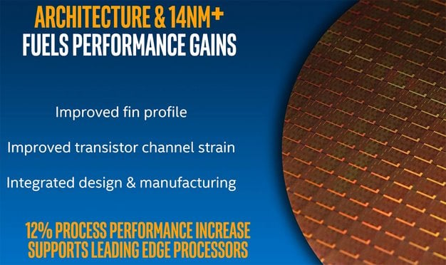
Intel 7th Gen Core Series Kaby Lake Wafer
If you’re unfamiliar with Kaby Lake, it is the follow-up product to last year’s Skylake. Kaby Lake borrows heavily from Skylake; its CPU cores, cache structure, and graphics engine are similar, and Kaby Lake is still manufactured using a 14nm process. There have been a number of enhancement made to Kaby Lake, however, that not only improve overall performance and efficiency, but enhance its multimedia capabilities and responsiveness as well.
Although Kaby Lake marks a departure from Intel’s tick-tock release cadence, there have been some tweaks made to its 14nm manufacturing process that have resulted in significant gains in performance. Intel is calling these new process optimizations "14nm+." Intel has tweaked the fin profile used in its tri-gate transistors to optimize the aspect ratio and pitch, and it has also improved the transistor channel strain. These changes have allowed Intel to significantly bump up the Turbo Boost clocks on Kaby Lake-based mobile processors over Skylake, while maintaining similar thermal and power envelopes.
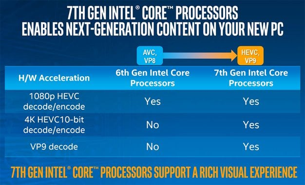
In addition to the tweaks made to the manufacturing process, Intel has incorporated a new multimedia engine into Kaby Lake that adds hardware acceleration for 4K HEVC 10-bit transcoding and VP9 decoding. Skylake could handle 1080p HEVC transcoding, but it didn’t accelerate 4K HEVC 10-bit transcoding or VP9 decode and had to assist with CPU resources.
The new multimedia engine gives Kaby Lake the ability to handle up to eight 4Kp30 streams and it can decode HEVC 4Kp60 real-time content at up to 120Mbps. And because all of this is handled in an efficient fixed-function engine, the low-power Y-Series Kaby Lake-based 7th generation Core series processors can also now handle 4Kp30 real-time encoding in a 4.5W package.
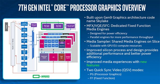
The graphics engine in Kaby Lake is essentially unchanged over Skylake, but due to the improved silicon process and transistor design, the GPU core is able to maintain higher clocks longer and it is also more power efficient. You’ll notice in the slide above, it’s only a small block at the top (circled in green) that’s marked as "improved" – that’s the multimedia engine we just mentioned.
In terms of its layout, the Kaby Lake die-map pictured here shows just how much real-estate is dedicated to CPU, GPU, and un-core resources. Dual CPU cores are in the middle, flanked by the graphics core below and system agent and memory controller above. The processor’s shared cache sits in between the CPU cores and all of the memory and I/O interfaces are off to the right.
On a side note, if you’d like to see a clean die-shot of Kaby Lake, we’ve got one posted in the high-res image gallery linked at the bottom of every page.


