|

 For
about three years now, a fierce battle has been raging
between Intel and
AMD.
This battle has taken consumers down a road that led to a
wider selection of higher performing processors than ever
before, and at prices that were much lower than previous
generations of flagship CPUs. As each company
introduced a new speed step, or introduced a new processor
core, the competition was right there to introduce their new
part in an effort to steal some thunder and make some noise
of their own. The Athlon arrived and quickly
became the first "mainstream" CPU to break the 1GHz barrier,
enticing a large part of the enthusiast community in the
process. Then Intel stepped up to bat and were the
first to reach the 2GHz mark. These two X86 rivals
have also been battling on price. With every press
release from AMD announcing their latest price cuts, came a
similar announcement from Intel. It seems that the
"one-upmanship" between these two companies will never end.
Today, only two months after introducing the Athlon XP
2000+, AMD unleashes their latest soldier, the Athlon XP
2100+. The core technology remains unchanged but the
clock speed has been bumped up another 66MHz, bringing AMD's
current flagship CPU to 1733MHz. What do you say we
get this CPU installed into one of our test beds and see
just what it can do? For
about three years now, a fierce battle has been raging
between Intel and
AMD.
This battle has taken consumers down a road that led to a
wider selection of higher performing processors than ever
before, and at prices that were much lower than previous
generations of flagship CPUs. As each company
introduced a new speed step, or introduced a new processor
core, the competition was right there to introduce their new
part in an effort to steal some thunder and make some noise
of their own. The Athlon arrived and quickly
became the first "mainstream" CPU to break the 1GHz barrier,
enticing a large part of the enthusiast community in the
process. Then Intel stepped up to bat and were the
first to reach the 2GHz mark. These two X86 rivals
have also been battling on price. With every press
release from AMD announcing their latest price cuts, came a
similar announcement from Intel. It seems that the
"one-upmanship" between these two companies will never end.
Today, only two months after introducing the Athlon XP
2000+, AMD unleashes their latest soldier, the Athlon XP
2100+. The core technology remains unchanged but the
clock speed has been bumped up another 66MHz, bringing AMD's
current flagship CPU to 1733MHz. What do you say we
get this CPU installed into one of our test beds and see
just what it can do?
|
|
|
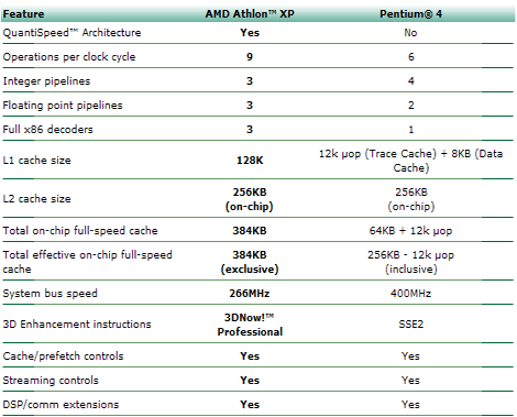
Specifications of the AMD Athlon XP 2100+
Processor |
|
A few more clock
cycles and some nice green packaging... |
|
CLICK IMAGES FOR ENLARGED
VIEW
Key Architectural Features of the AMD Athlon? XP Processor:
-
QuantiSpeed?
Architecture for enhanced performance
-
Nine-issue
superpipelined, superscalar x86 processor
microarchitecture designed for high performance
-
Multiple
parallel x86 instruction decoders
-
Three
out-of-order, superscalar, fully pipelined floating point
execution units, which execute x87 (floating point), MMX?
and 3DNow!? instructions
-
Three
out-of-order, superscalar, pipelined integer units
-
Three
out-of-order, superscalar, pipelined address calculation
units
-
72-entry
instruction control unit
-
Advanced
hardware data prefetch
-
Exclusive and
speculative Translation Look-aside Buffers
-
Advanced
dynamic branch prediction
3DNow!? Professional technology for leading-edge 3D
operation:
-
21 original
3DNow!? instructions?the first technology enabling
superscalar SIMD
-
19 additional
instructions to enable improved integer math calculations
for speech or video encoding and improved data movement
for Internet plug-ins and other streaming applications
-
5 DSP
instructions to improve soft modem, soft ADSL, Dolby
Digital surround sound, and MP3 applications
-
52 SSE
instructions with SIMD integer and floating point
additions offer excellent compatibility with Intel's SSE
technology
-
Compatible
with Windows® XP, Windows 98, Windows 95, and Windows NT®
4.x operating systems
266MHz AMD Athlon? XP processor system bus enables excellent
system bandwidth for data movement-intensive applications:
-
Source
synchronous clocking (clock forwarding) technology
-
Support for
8-bit ECC for data bus integrity
-
Peak data rate
of 2.1GB/s
-
Multiprocessing support: point-to-point topology, with
number of processors in SMP systems determined by chipset
implementation
-
Support for 24
outstanding transactions per processor
Other Architectural Elements:
-
The AMD Athlon?
XP processor with performance-enhancing cache memory
features 64K instruction and 64K data cache for a total of
128K L1 cache. 256K of integrated, on-chip L2 cache for a
total of 384K full-speed, on-chip cache.
-
Socket A
infrastructure designs are based on high-performance
platforms and are supported by a full line of optimized
infrastructure solutions (chipsets, motherboards, BIOS).
Available in Pin Grid Array (PGA) for mounting in a
socketed infrastructure Electrical interface compatible
with 266MHz AMD Athlon XP system buses, based on Alpha
EV6? bus protocol
-
Die size:
approximately 37.5 million transistors on 128mm2.
Manufactured using AMD's state-of-the-art 0.18-micron
copper process technology at AMD's Fab 30 wafer
fabrication facility in Dresden, Germany.
| To
demonstrate the main features differentiating the AMD
Athlon XP from Intel's Pentium 4, this table from AMD's
marketing team breaks things down for you. The
table is a bit dated though, as it lists features foe a
"Willamette" based Pentium 4 that only has 1/2 of the
amount of cache as the new Northwood Pentium 4 that is
also currently available.
AMD has
dubbed the combination of enhancements and features
found in the Athlon XP line of CPUs, their "QuantiSpeed"
Architecture. So, what exactly is "QuantiSpeed"
all about? We'll let AMD tell the story.
QuantiSpeed? Architecture:
QuantiSpeed? architecture allows the AMD Athlon? XP
processor to accomplish more instructions per clock
cycle (IPC). Improved IPC is a result of the following
technological advances.
Nine-issue, superscalar, fully pipelined
microarchitecture:
Provides more pathways to feed application
instructions into the execution engines of the core,
allowing the processor to complete more work in a given
clock cycle (high IPC). The delicate balance between the
depth of the pathways and clock speed of the processor
produces high levels of performance.
Superscalar, fully pipelined
Floating Point Unit (FPU):
Completes more floating point operations per
clock cycle than competitive x86 processors and permits
high operating frequencies. The end result is a
processor with the computing power to tackle the most
computation-intensive software applications.
Hardware data prefetch:
Prefetches data from system memory to the
processor's Level 1 cache, which reduces the time it
takes to feed the processor critical data, increasing
work throughput and therefore overall performance.
Exclusive and speculative
Translation Look-aside Buffers (TLBs):
Keep the maps to critical data close to the
processor, which helps prevent the processor from
stalling or waiting when future data is requested. These
TLB structures are now larger, exclusive between caches,
and speculative. Larger TLB's give the AMD Athlon XP
processor access to additional data maps. Exclusivity
removes the duplication of information, freeing up more
space in the Level 2 cache for other useful data to be
used by the processor. And the speculative nature of
these structures allows the processor to generate future
maps of critical data quickly.
These four key advances
allow AMD's QuantiSpeed architecture to perform more
calculations per second, boosting overall throughput.
|
Processor ID and Preliminary Tests
|
 For
about three years now, a fierce battle has been raging
between Intel and
For
about three years now, a fierce battle has been raging
between Intel and