


Qualcomm Validates HBC Silicon With Huge 18x Leap In AI Memory Bandwidth


Computing demands have been changing as LLMs transition from training to large-scale agentic inference, specifically how the latter is bound primarily by memory bandwidth, or rather, how rapidly weight and activation data can traverse the physical space between memory pools and processing units. While high bandwidth memory (HBM) is the current go-to solution, HBM incurs steep thermal, financial, and electrical power premiums due to off-package data movement over millimeter distances. SRAM-based alternatives offer massive throughput but falter on memory capacity and total cost of ownership at rack scale.

Physical validation on automated test equipment in San Diego confirmed that the core technology functions as intended under production-representative dimensions using randomized weights and activations. Hardware measurements showed that first-gen HBC achieves an 18-fold increase in effective memory bandwidth compared to LPDDR5X memory implementations. On the energy-efficiency front, HBC delivered over five times the bandwidth-per-watt performance of projected HBM4 specifications. Indeed, the latter score came in slightly below the company's initial 6-fold projections, but still, it's quite the win.
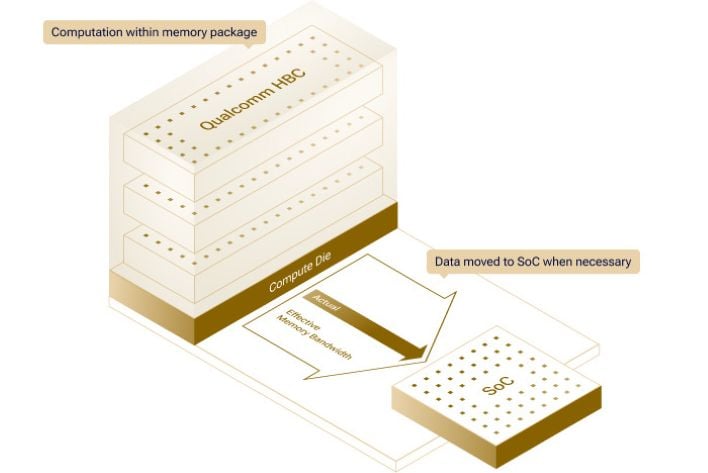
Qualcomm plans to commercialize HBC technology within its Dragonfly AI portfolio. The first product, the Dragonfly AI250 accelerator platform, is scheduled to sample to enterprise customers and hyperscalers in the first half of 2027. Made for disaggregated inference workloads, a full Dragonfly AI250 liquid-cooled rack sports 38.6TB of system memory capacity and 7.4 petabytes per second of effective memory bandwidth. The company also plans to deploy its custom Oryon-based C1000 server CPU in 2027, followed by next-gen HBC integration in the Dragonfly AI300 platform in 2028.