Intel Shows Off Bottleneck-Busting PowerVia Tech, On Schedule For 2024 Arrival
Well, if we apply this same idea at a lower level, there's an obvious target for decoupling: the signal and power wires inside the microprocessor itself. As Intel explains it, processors are traditionally created like building a pizza, stacking on layers that aggressively scale in pitch, or size. This means that signalling and power delivery have to compete for resources (like area and thermal limits) at every metal layer within the chip.
Moving the power delivery circuitry to the back side of the chip simplifies things a lot, and it offers improved performance as well as reduced manufacturing cost, but there are lots of issues this approach, too. After all, it's not a completely novel idea—Intel's own work on the concept began over a decade ago. The thing is, we've reached a point in transistor scaling where the gains from a "Back Side Power Delivery Network" (BS-PDN) are too great to ignore.
As Intel's slide admits, the biggest risks associated with backside power delivery are worse yields, reduced reliability, hampered thermal dissipation, and crippled debug capability. Naturally, Intel says that it has overcome these challenges in its first working implementation of BS-PDN, known as PowerVia.
So, what's so clever about PowerVia compared to previous backside power delivery concepts? It's the use of a thing that Intel calls "Nano TSV". TSV of course stands for "through-silicon via" and you should be familiar with the term by now, as it's the way that stacked chips (like AMD's 3D V-Cache) are connected. Nano-TSVs are, according to Intel, five-hundred times smaller than typical TSVs.
These are used to deliver power straight to the M0 layer where the processing actually happens rather than having to pass through the M0 layer. This greatly simplifies things, and it allows Intel some breathing room on that layer as it doesn't have to account for extra power routing mucking up the signaling above the M0 layer.
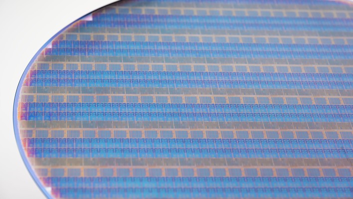
These test chips are known as "Blue Sky Creek" and are simple processors with just a pair of Crestmont E-core clusters. Intel didn't talk about the performance or capabilities of Blue Sky Creek; it's unlikely that these chips will ever find their way into any production system. The point is that these chips are fabricated using Nano TSVs connected to BS-PDN and that it all works as expected.
However, Intel did provide some numbers for us to salivate over: a 30% reduction in voltage droop means that chips can use lower voltage to begin with, improving efficiency and reducing power consumption. This comes along with a 6% increase in the maximum achievable core frequency, which sounds small, but isn't bad at all considering we're fundamentally talking about the same Intel 4 manufacturing process. Increasing clocks by 6% with lower power and no die shrink is pretty good.
As far as yields go, well, they're worse—but Intel says that yields on this modified Intel 4 process have been tracking behind yields on the standard Intel 4 process by about two quarters. In other words, the defect rate is trending down, which means that Intel's foundry is figuring out how to make these chips with fewer defects. According to the chart in Intel's slide, it looks like the defect rate now is only slightly worse than on the standard Intel 4 process.
Finally, as far as thermals go, Intel has taken significant measures to deal with the fact that there's now silicon between the transistors and the heatspreader or cooling apparatus. The slide above says that thermal response is "in line with power density increase expected from frequency scaling." In other words, it says that thermal response of these chips isn't actually worse than that of standard Intel 4 processors.
That does appear to be mainly down to Intel's measures to prevent thermal response from being terrible, and those measures, if we're understanding Intel's slide correctly, include some 30% of the core area being devoted to structures intended to improve thermal transfer.
In any event, Intel is rightfully stoked about the manufacturing success, and says that PowerVia will be used on RibbonFET processors manufactured on the company's 20A and 18A process nodes. As planned, those chips will apparently start showing up next year. If it succeeds, Intel will be ahead of the game for sure, as neither TSMC nor Samsung are expected to have backside power delivery ready before 2026.


