NVIDIA GeForce RTX 2080 Ti NVLink SLI Scaling Explored
There are a couple of polished, hex screws visible on the top of the NVLink bridges, which look they may just be decorations, but there are functional and need to be removed to pull apart the bridge.

Top and Bottom Shell
Inside the shell, the metal retainer nuts are visible both top and bottom, along with an array of reinforcements and the wiring and connector for the LEDs that reside in the bridge.

Inside the NVLink Bridge Shell
There is a 5-pin cable leading to the lighting on the top, which illuminates the NVIDIA logo visible at the center. NVIDIA hasn't specified whether or not its bridges are RGB capable, but the 5-pin lead is overkill for a simple LED and hints that some sort of control and customization may be possible, especially since boards partners have RGB NVLink bridges available.
The top of the NVLink PCB has a few surface mounted components over an above simple filters to keep the signaling clean. NVIDIA hinted that NVLink lays the foundation for additional features and functionality, which is perhaps by these bridges are so much more complex than what was used with traditional SLI.
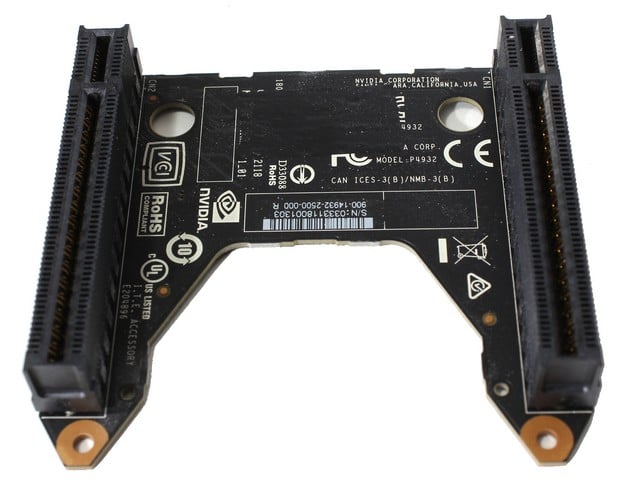
Viewing the bridge from the bottom we see the two connectors which very strongly resemble a PCIe slot. While the connectors do a PCIe slot the smaller section, which would normally be used for power on a PCIe slot, is smaller. Interestingly, part of the PCB was also covered with electrical tape, which we promptly removed.
Removing the tape reveals solder pads for an SMD device. We are not sure what it could be used for, but we may revisit this at some point after scoping the PCB/pins and seeing what kind of continuity we get and to what parts/controllers they're connected to.
It is worth mentioning that the MPN listed on the PCB "NVA-P4932" does coincide with a FCC listing for an "NVLink 2 Bridge", applied on 8/30/2018, so this is definitely not just a re-badged professional unit in-line with what is used on Quadro cards.
Short of an ARM-based micro-controller, there's not much to see on the NVLink PCB. There is an array of surface mounted components and traces, but overall it is relatively simple.
Now that we've seen what the NVLink bridge is all about, let’s strap these to the bench and see how a couple of GeForce RTX 2080 Ti card perform when linked up for SLI...


