TSMC Details Cutting-Edge 1.4nm Chip Node With Big Speed And Efficiency Gains
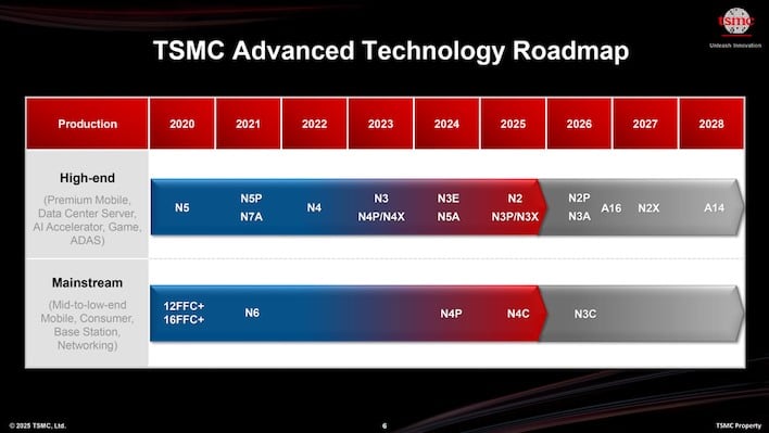
Let's talk about the state of TSMC's current offerings. You've got N3P and N3X, which are high-power-optimized and max-power-optimized versions of the company's popular N3 process. You've also got N2, which is the current state-of-the-art, at least at TSMC. Next up on the docket are N2P and N3A, with the former being a power-optimized version of N2, and the latter being a modification of N3 for absolute maximum yield rates.
A16 will come after, but A16 is an interesting name for what is really N2P with TSMC's "Super Power Rail" back-side power delivery network (BSPDN.) This is analogous to Intel's PowerVia, and like that technology, A16 promises to offer increased density and efficiency over N2P. However, it will also bring along increased manufacturing complexity as well as unresolved thermal challenges, so confusingly, TSMC is NOT planning to use Super Power Rail on its A14 process. Instead, that will come later.
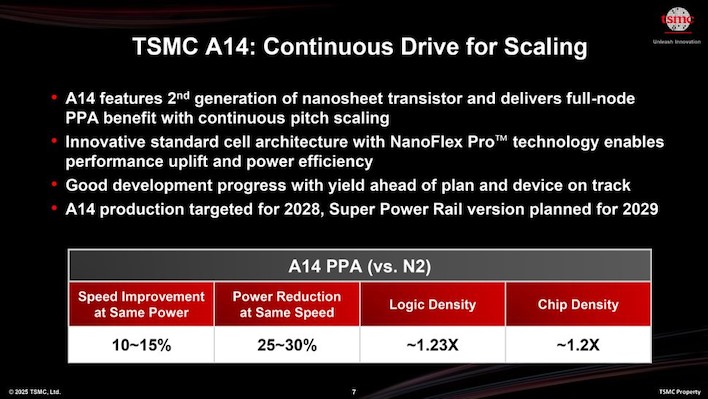
A14 should still be a considerable improvement over N2, though. TSMC is claiming that the new process will offer as much as a 30% drop in power at iso clocks, or a 15% gain in performance at iso power versus N2. It also apparently offers a 20% gain in transistor density versus the previous main-line manufacturing process. Those sorts of benefits are pretty good considering the extremely small changes in absolute dimensions; TSMC calls the gains in Performance, Power, and Area (PPA) are "full-node," which is arguable from both sides.
TSMC says that it plans to have A14 in the volume production stage in 2028, while the enhanced version with the Super Power Rail BSPDN feature will show up the next year, in 2029. That's five years away, but it really goes to illustrate how long in advance these things have to be planned. In the meantime, we're keen to see how TSMC's A16 compares to Intel's A18 given that both are using GAAFETs and BSPDN.


