AMD EPYC Is First In TSMC N2 But Intel 18A Could Be Stiff Competition
First up, AMD's next-generation EPYC processors, code-named "Venice" and thought to be using Zen 6 CPU cores, are among the very first marketable chips to roll off of TSMC's newest fabrication tech. The CPUs are being made in Taiwan and expected to launch next year, although AMD also notes that its extant 5th-gen EPYC processors, codenamed "Turin", are also coming off the N3 fab node at TSMC's Arizona plant.
As Intel has lagged behind TSMC in manufacturing for nearly a decade now, it's surprising to hear that the latest buzz in of the beehive of industry speculation that Intel's upcoming 18A process may in fact be superior to both TSMC and Samsung's efforts. 3C News reports that TechInsights rated the performance of Samsung SF2, TSMC N2, and Intel's 18A on an internal scale, coming up with values of 2.19, 2.27, and 2.53, respectively.
What this means essentially, is that Intel's 18A process offers superior performance-per-watt compared to Samsung and TSMC's efforts. That could translate directly into improved efficiency or performance for Intel's processors manufactured on that node (or both), although the quality of the node is only one factor these days, in the world of advanced packaging and multi-chiplet CPUs. Still, Intel hasn't had a truly competitive process since the days of 14nm, so this is very good news for the blue team. And indeed Intel's packaging prowess is also well established as well.
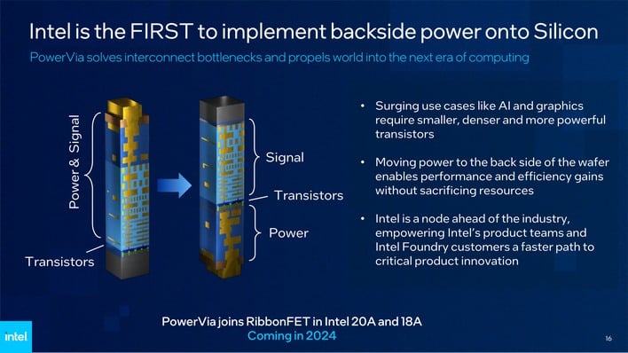
Intel's 18A process comes with a lot of technological advancements behind it that are driving these gains. 18A implements Intel's RibbonFET Gate-All-Around (GAAFET) design, and it also brings the PowerVia backside power delivery network, which is a first in the industry. According to Intel, 18A offers a 15% improvement in performance-per-watt over its extant Intel 3 process, and a whopping 30% improvement in density, meaning more transistors can be packed into the same die area.
But what about yields? 3C News quotes KeyBanc as saying that yields in terms of defect density have "reached acceptable standards," and that the process overall is "indeed excellent." Vinh apparently also thinks that Intel could have a shot at manufacturing the processors for a potential third-generation Nintendo Switch. That'll be at least five or six years away from now, though, so only time will tell.


