Back in the 1990s, NVIDIA got its start selling graphics adapters for desktop PCs. After a rocky start with the NV1,
NVIDIA established itself as a performance leader soon thereafter with the release of the TwiN-Texel (TNT) chip, and with the original GeForce 256, as a technology leader, too.
That's all ancient history now, but the facts haven't changed: NVIDIA is the world's biggest producer of discrete graphics processors. People usually simply say "GPUs," yet that's become a bit of an ironic name as the years go on. Team Green still sells lots of graphics chips, of course, but the biggest portion of its revenue comes from repurposing these "GPUs" as massively-parallel compute accelerators. In fact, one could reasonably argue that the chips are intended for the compute market, and being "repurposed" for the graphics business.
Of course, neither statement is exactly accurate, but either way, it's true that compute workloads and graphics workloads want different things from a processor. It's likely for this reason that it seems NVIDIA is moving away from its firm "one architecture at a time" stance toward operating at least two different designs in parallel. That's happened in the past; look at Kepler and
Maxwell, or Pascal and Volta. This time it seems more official, though; NVIDIA's new chip seems to be a more direct replacement for Ampere in the datacenter.
Indeed, as part of an all-out assault of announcements at
GTC today NVIDIA revealed its next-generation "big" GPU,
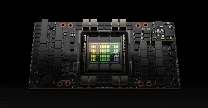
Hopper H100. Those who follow GPU rumors will correctly surmise that H100 is based on the Hopper architecture, and if you're into AI, you'd better sit up, because this is a very, very big deal.
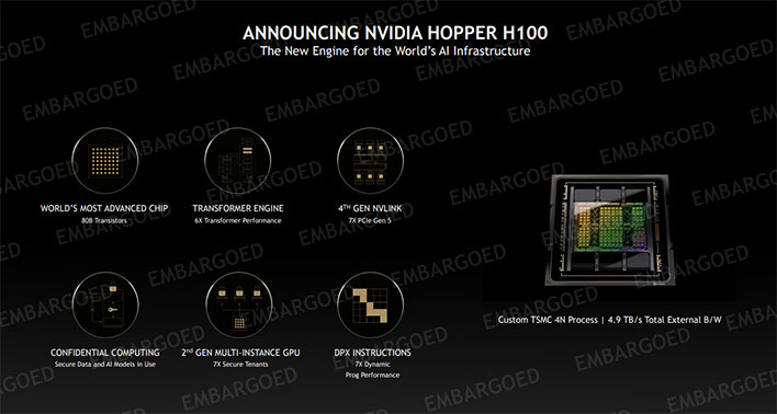
NVIDIA's new H100 is fabricated on TSMC's 4N process, and the monolithic design contains some 80 billion transistors. To put that number in scale, GA100 is "just" 54 billion, and the GA102 GPU in the
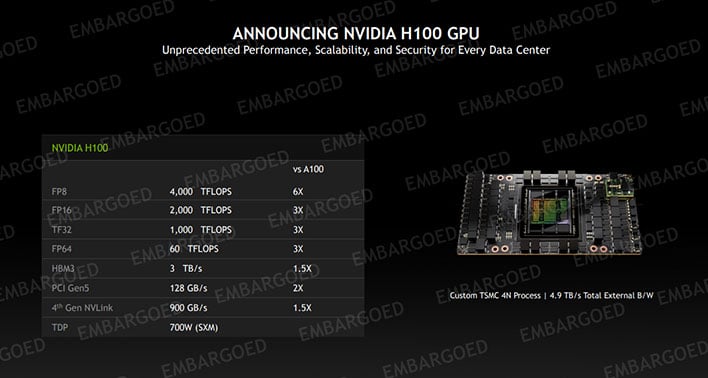
GeForce RTX 3090 is a measly 28.3 billion. Despite being such a massive processor, and despite being fabricated on the absolute bleeding edge of microprocessor process technology, the TDP for the SXM (mezzanine) version of the chip is seven-hundred Watts. Yeah, 700.
Those dizzying numbers bring in similarly-shocking performance comparisons. The company claims that an H100 chip eclipses its previous-generation
A100 processor by a factor of three in double-precision compute, single-precision tensor compute, and half-precision compute, while being fully six times faster at 8-bit floating point math.
The move to HBM3 memory improves the per-pin transfer rate from 2.43Gbps to 4.8Gbps, but otherwise the memory configuration is unchanged: five active stacks of HBM3 (with one dummy) giving a total capacity of 80GB per GPU and total bandwidth of 3TB/sec. The GPU's NVLink connection steps up to the 4th generation, too, resulting in 900GB/sec bandwidth between the GPU and its host system. For products that don't use
NVLink, H100 also implements PCIe 5.0.
As far as the GPU itself goes, the full implementation of GH100 features the following specs...
- 8 GPCs, 72 TPCs (9 TPCs/GPC), 2 SMs/TPC, 144 SMs per full GPU
- 128 FP32 CUDA Cores per SM, 18432 FP32 CUDA Cores per full GPU
- 4 Fourth-Generation Tensor Cores per SM, 576 per full GPU
- 6 HBM3 or HBM2e stacks, 12 512-bit Memory Controllers
- 60MB L2 Cache
- Fourth-Generation NVLink and PCIe Gen 5
And the H100 GPU with SXM5 board form factor boasts the following...
- 8 GPCs, 66 TPCs, 2 SMs/TPC, 132 SMs per GPU
- 128 FP32 CUDA Cores per SM, 16896 FP32 CUDA Cores per GPU
- 4 Fourth-generation Tensor Cores per SM, 528 per GPU
- 80GB HBM3, 5 HBM3 stacks, 10 512-bit Memory Controllers
- 50MB L2 Cache
- Fourth-Generation NVLink and PCIe Gen 5
NVIDIA also said Hopper includes new instructions known collectively as "DPX." These instructions are intended to accelerate dynamic programming, and NVIDIA says that code using them can achieve speedups of up to 40x, but that comparison is a little murky; rather than against last-generation's A100, NVIDIA is comparing four H100 chips against a pair of 32-core Ice Lake Xeons.
The company also says that its compute cores include a "Transformer Engine" that can be used to accelerate Transformer-type neural networks by "as much as 6x" versus Ampere. The "Transformer Engine" itself seems to be marketspeak for tweaked tensor units that, in combination with smart software, can step operations all the way down to 8-bit precision when higher precision is not required.
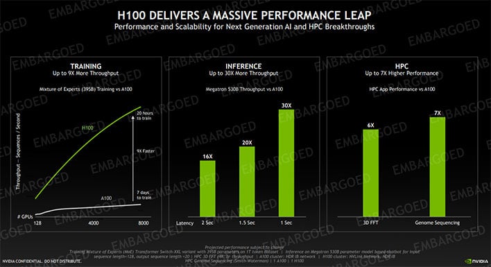
It's this capability that allows the H100 to achieve its greatest performance gains compared to the Ampere-based A100, according to NVIDIA. For AI model training, the H100 can apparently achieve 9x the throughput. For AI inferencing, the gains are even larger; NVIDIA claims that per-GPU throughput with H100 is fully thirty times that of A100 with a 1-second response latency.
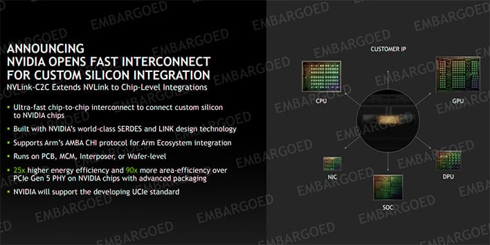
Stepping back to NVLink and PCIe for a moment, the latest offshoot of NVIDIA's interconnect is called NVLink-C2C. C2C stands for "chip to chip", and it indicates that this version of NVLink is intended for use with both GPU-to-host connections as prior versions of NVLink, but also between dice in "advanced packaging."
Basically, it's another interconnect that can be used between chiplets, similar to (but much faster than) AMD's Infinity Fabric. It's used in the Grace Superchip and Grace Hopper Superchip, also announced today, and NVIDIA says it is "open for semi-custom silicon-level integration with NVIDIA technology." NVIDIA's also supporting UCIe (
Universal Chiplet Interconnect Express), by the way.
In its release materials, NVIDIA states multiple times that H100 "can be deployed in every type of datacenter." That's because the company is offering H100 in numerous form factors, ranging from a specialized PCIe add-in card all the way up to pre-configured supercomputer blueprints with 256 H100 GPUs.
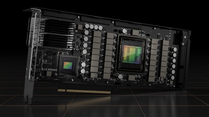
The most basic form of H100 will be the mezzanine version in SXM form factor, but as an add-in card it will come as the H100 CNX "Converged Accelerator." Basically, the card includes an H100 GPU as well as one of NVIDIA's own ConnectX-7 dual-port Infiniband adapters. The GPU connects to the NIC using PCIe 5, while the NIC connects to the host using PCIe Gen 4. The idea is that it's more important for the accelerators in a node to be able to talk to each other with the lowest latency and highest throughput possible.
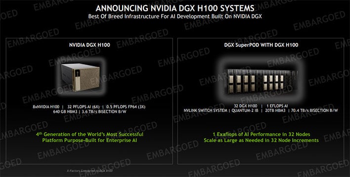
Naturally, there's a new DGX system to accompany this launch, christened DGX H100. This fourth generation of NVIDIA's supercomputing module is extremely similar to the
previous-generation DGX A100; mostly, it swaps out the eight A100 GPUs for eight SXM H100 accelerators, giving it fully 32 petaFLOPS of 8-bit compute. The DGX SuperPOD, then, combines 32 DGX systems for a total of 1 exaFLOP of AI inferencing horsepower.
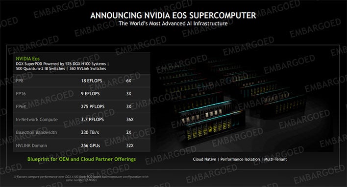
NVIDIA says that the latest DGX SuperPOD will allow its supercomputing customers to "scale as large as needed in 32-node increments." Indeed, that seems to be the basis for the Eos Supercomputer blueprint which piles together some 18 SuperPODs, comprising 576 DGX H100 systems, linking together 4,608 H100 GPUs.
None of this is coming to retail, of course. Despite NVIDIA's claims that it wants H100 "at every scale," most of the products in this announcement are really aimed squarely at governments and large research organizations (generally subsidized by governments) that need the absolute maximum in number-crunching compute power. As such, NVIDIA didn't provide any pricing data. All of these products are in "if you have to ask, you can't afford it" territory.
The House That GeForce Built did say that H100 is in production already, and gave a date for availability of these products, too. If you're after the latest and greatest in AI acceleration hardware, start pinging your vendor in Q3 of this year.

