Intel Foveros To Usher In Industry First 3D Stacked System On A Chip Designs
Intel held an Architecture Day in Los Altos yesterday, where it disclosed a number of details regarding next-generation CPU and GPU architectures and manufacturing process technologies. In addition to the technical disclosures divulged to an exclusive group of attendees, Intel also talked about a shift in the company’s design and engineering model based on six strategic pillars -- Process, Architecture, Memory, Interconnect, Security, and Software – which it hopes will allow it to better address the needs of the current computing landscape moving forward.
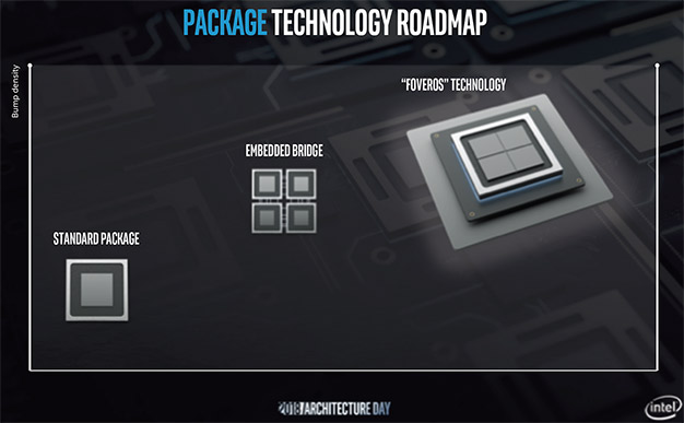
In addition to the architecture and roadmap news, Intel also talked about a new, very interesting 3D packaging technology it is calling “Foveros”, which will allow for the industry’s first 3D stacking of complex logic.
Now, 3D stacking and 3D integrated circuits are not new technologies; they have been employed for years. Foveros, however, is something different. Foveros takes things a step further and will enable logic-on-logic integration. Foveros goes beyond traditional die stacking with passive interposers and stacked memory and will work with high-performance logic circuits, like CPU cores, GPUs, AI processors, and the like.
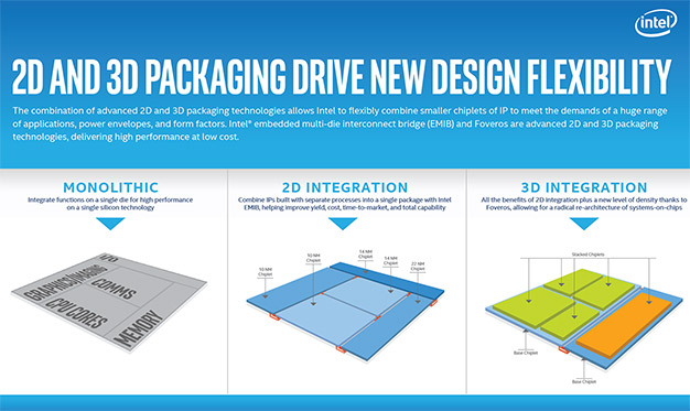
Because of its unique capabilities, Foveros should usher in some interesting chip designs. For example, with Foveros, both high-performance / high-density and low-power silicon can be combined on a single device. As such, in conjunction with Intel’s EMIB (Embedded Multi-die Interconnect Bridge) 2D packaging technology, Foveros will allow designers to mix-and-match IP blocks with various memory, sensor, and I/O elements, to create new devices and form factors.
With Foveros and EMIB, devices comprised of smaller “chiplets,” with SRAM, I/O, and power delivery circuits, can all be parts of a base die, and additional high-performance logic chiplets can be stacked on top via high-bandwidth silicon vias.
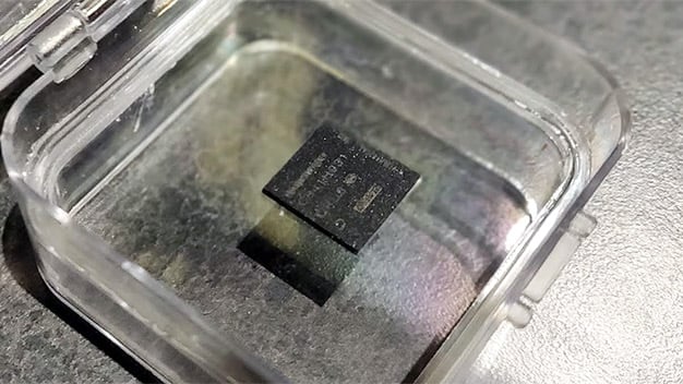
According to Intel, it expects to launch a range of products that leverage Foveros, starting in the second half of 2019. The first Foveros-based product, which was actually demoed live at the event, will combine a high-performance 10nm compute-stacked chiplet with a low-power 22nm base die.
The next-gen SoC shown at Intel's event was comprised of 5 cores in total – four low-power efficiency cores and one high-performance core – with graphics, I/O, and POP memory all in a single 12x12x1mm chip that uses only 2mW of power in standby. The demo showed 4K video being played back and scaled down to 1080p on the low-power core, under Windows 10, with low CPU utilization. Resizing the video (or pressing the Windows key) seamlessly un-parked the high performance core, but no other benchmarks or performance data was disclosed.
All told, Foveros and EMIB will allow Intel to not only mix-and-match chiplets produced with different process technologies, to improve yields, cost, and time-to-market, but to also pack them in multiple dimensions onto single devices, to increase density and enable new form factors. The technologies seemed promising and seeing devices already up and running was encouraging, to say the least.


