PS5 Pro Specs Revealed As Teardown Shows Improved Repairability
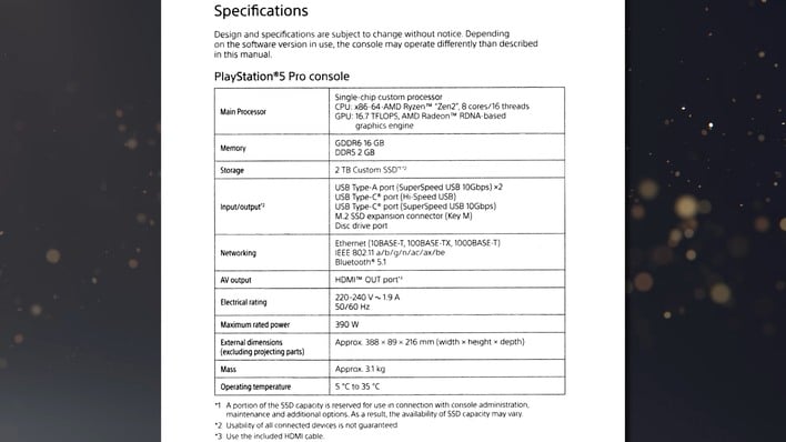
The unboxing was not particularly momentous (as they rarely are), but hosts Leadbetter and Linneman were equally surprised at the fact that the PS5 Pro is actually a touch smaller than the original PS5. The really interesting part was buried in the safety manual for the device, though. Richard Leadbetter noticed that there are, unusually, full specifications for the system hidden away in the booklet.
There's not much here that's a surprise, especially after we saw so many early leaks about the machine's hardware, but those very same leaks did mislead us on one critical spec: the GPU performance. Sony quotes the processing power of the PS5 Pro's GPU at 16.7 TFLOPS, which is roughly half of the 33 TFLOPS rumored in pre-launch leaks. Does that mean the PS5 Pro is much weaker than expected?
Well, probably not, no. You see, the difference here is almost certainly down to the dual-issue capability of RDNA 3 graphics processors. The GPUs in the PS5 and indeed the PS5 Pro are not based directly on any AMD discrete GPU architecture, but rather closely related to commercial AMD graphics processors, and the PS5 Pro's GPU was expected to preserve the dual-issue capability of RDNA 3. It seems like that may not be the case, though.
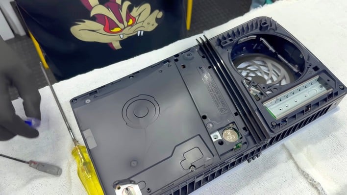
The other notable bit of PS5 Pro news today is that Brazilian YouTube channel TAG are the first on the 'net to tear down a PS5 Pro, taking the machine apart to show its innards. Much like with the unboxing, there's a whole lot of "yep, that's the inside of a PS5 Pro," but there are a couple of key takeaways. First and foremost is the presence inside the outer shell of an easy slot to access the machine's CMOS battery.
This is nearly unheard-of in game consoles, and an extremely welcome change, as it dramatically increases the machine's repairability. With many earlier consoles, if the CMOS battery was even removable without desoldering, it would have been hidden under a heatsink that required removing a dozen screws to access. Here, you can simply pop off the top cover of the PS5 Pro and easily get to the system's CMOS battery, which is a boon for preservation.
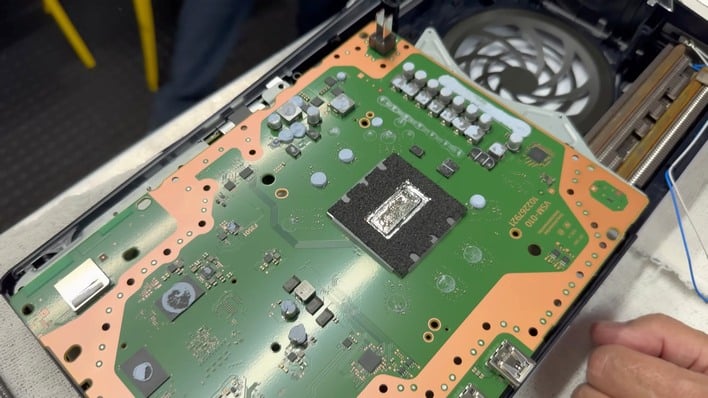
Another interesting quirk is that Sony is still using liquid metal thermal interface material (TIM) on the PS5 Pro's SoC. Some had rumored that the company would move away from liquid metal TIM after the dangerous material—dangerous to electronics, not to humans—had leaked in a few units during shipping. Clearly the thermal transfer benefits of the expensive TIM are way too good to ignore, and TAG has to be careful manipulating the motherboard and cooler to avoid spilling the precious TIM.


