Nvidia Announces GeForce GTX 680M, Unveils Obtuse Product SKUs
Comparative performance in 3DMark 11 Performance Preset Source -- Nvidia

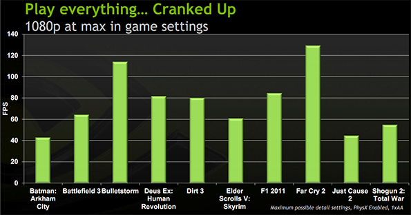
GTX 680M performance in an array of modern titles. Source - Nvidia
Nvidia also claims a number of wins over AMD's HD 7970M, but the company provides no configuration information or game test data to back up its claims. As a result, we've not reproduced them here.
In the grand scheme of things, the 28nm flavors in the 600-series lineup are extremely well-positioned. If Intel's ultrabooks take off -- and the CPU manufacturer is dedicated to ensuring that they do -- Nvidia has a product family of extremely power-efficient GPUs it can position as complementary upgrades. If ultrabooks don't take off, NV still wins points for Kepler's improved performance/watt. Without an integrated CPU+GPU, and with ARM-based tablets/netbooks running Windows 8 still at least nine months away from the mass market, NV needs to keep itself on the cutting-edge of mobile GPU technology -- and it looks to have nailed that this time around.
Less Stack, More Rickity Staircase
In the past, we've criticized AMD for choosing to split the HD 7000 family (both desktop and mobile) between 40nm, rebranded HD 6000 hardware and new 28nm parts built on the company's Graphics Core Next. Unfortunately, Nvidia decided to one-up its competitor in the worst way possible. When AMD split the HD 7000 Mobility family, it did so by model number -- HD 7700 - HD 7900 cards all use 28nm technology, everything below that is built on 40nm.
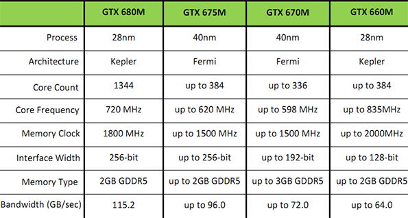
Nvidia, in contrast, is all over the map. The GTX 680M is a 28nm Kepler part. The GTX 675M and 670M are both 40nm Fermi, while the 660M, 650M, and 640M are all Kepler. The 640M LE family is listed as both Kepler (28nm) and Fermi (40nm) while the 635M, 630M, and 620M include 28nm Fermi options as well as the standard 40nm flavor.

The high-end chips are a bit confusing, but not too much. Again, the GTX 680 can address 4 GB of RAM

In the midrange, it's markedly less clear.
To summarize: Kepler is 28nm and Fermi is 40nm, except when Fermi is also 28nm. Kepler and Fermi are both mostly DDR5, but there are DDR3 options at the low end. Cards are limited to 2GB of RAM, except for the 670M, which is a 40nm GPU with a 3GB option. Finally, the GT 635M packs a full 384 Fermi cores -- as many as the GTX 675M -- but offers only 50% the memory bandwidth of that card.
Although not shown here, the low-level GT 630/620M families are all Fermi parts -- but there's a marked difference in clock speed due to the process technology difference. The 40nm Fermi chips are clocked at 752MHz (630M) and 475MHz (620M) while the 28nm chips are clocked at 800MHz and 625MHz, respectively. This means that while the performance difference in the 630M family is fairly small, the 28nm 620M Fermi will outperform the 40nm version by a significant amount.
We had a long talk with Nvidia regarding these product positions and our concerns that the widely varying specs could confuse customers. Nvidia claims that its model numbers are set to give customers an idea of what performance will be, even in cases where the underlying specs are quite different. Absent any hardware to test, we'll have to hope that the company bet correctly this time around.

