AMD Ryzen 9 9950X3D Spotted With A 5.65GHz Clock Speed And 128MB L3 Cache

AMD made some key changes to its second generation 3D V-Cache design that allows it to be more flexible with clock speeds, and rumor has it that both the upcoming Ryzen 9 9950X3D and Ryzen 9 9900X3D will feature the same top speeds as their non-X3D counterparts. While still not official, a leaked CPU-Z screenshot seemingly confirms that this will be the case, at least on AMD's upcoming flagship CPU.
The rumor first gained traction last weekend when HXL (@9550pro) on X/Twitter referenced both unreleased processor models on the social media site, saying there would be "no frequency debuff" on AMD's Zen 5-based chips with 3D V-Cache.
To an extent, we already saw some top-end 'frequency debuffing' with AMD's Ryzen 7 9800X3D, its first consumer Zen 5 processor to feature 3D V-Cache. We say "to an extent" because there does not exist a regular Ryzen 7 9800X. The closest approximation is the Ryzen 7 9700X. Here's how the chips compare:

The Ryzen 7 9800X3D is an 8-core/16-thread part with a 4.7GHz base clock, up to a 5.2GHz boost clock, and 96MB of L3 cache. Meanwhile, the Ryzen 7 9700X is also an 8-core/16-thread chip, but with a lower 3.8GHz base clock, higher 5.5GHz max boost clock, and 32MB of L3 cache.
Looking ahead, the Ryzen 9 9950X3D and Ryzen 9 9900X3D both have model-tier equivalents without 3D V-Cache bolted on, which raises the question of where clock speeds will land. Well, if recent leaks are accurate, they'll be same (or roughly the same), just as HXL said.
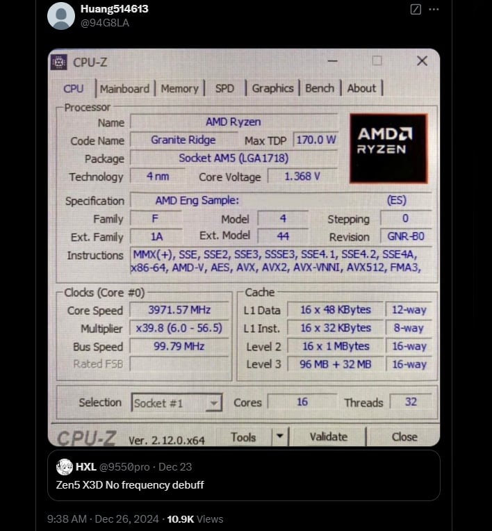
Over on X/Twitter, user Huang514613 (@94G8LA) posted a CPU-Z screenshot purporting to show vitals for the soon-to-be-announced Ryzen 9 9950X3D. The screenshot identifies the chip as an engineering sample with 16 cores and 32 threads, as one would expect.
More interesting is the multiplier section. Assuming the screenshot is legit, the ES chip has an unlocked multiplier range of 6.0 to 56.5x, which works out to a top clock of around 5.65GHz (or 5,638.135MHz with the reported 99.79MHz bus speed). Close enough to 5.7GHz, right?
What's also interesting is the L3 cache identification. The screenshot suggests a dual-CCD (core complex die) arrangement with 32MB of L3 cache on both dies, plus another 64MB of 3D V-Cache on one of the dies (hence 96MB), for a total of 128MB of L3 cache.
Engineering samples are not always indicative of a chip's final specs, and being a leak, the usual disclaimers apply (basically boils down to, take this with a grain of salt). That said, there's nothing wild here, and the screenshot is in line with previous leaks.
