AMD Zen 3 Ryzen, Threadripper And EPYC 7nm+ CPUs May Get Huge Transistor Density Uplift

AMD is on the cusp of releasing a new generation of Ryzen processors based on its 7-nanometer Zen 2 architecture, and from everything we have heard to this point, it is going to be an exciting launch. Looking beyond Zen 2, however, is where things may get truly interesting, as AMD's Zen 3 architecture transitions to a 7nm+ extreme ultraviolet lithography (EUV) manufacturing process.
Each new generation should bring a jump in IPC (instructions per clock) performance and better power efficiency, and we certainly expect that to be the case with Zen 2, and later Zen 3. What's interesting about Zen 3, though, is it will be the first semiconductor design to incorporate Taiwain Semiconductor Manufacturing Company's advanced EUV process in volume.
The use of EUV allows for finger circuit patterns. It is a short wave light source that, grossly simplified, creates tiny patterns on wafers. This in turn means the ability to pack more transistors into a smaller space.
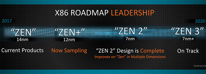
AMD's Zen 3 chips produced on a 7nm+ EUV node are on track for a 2020 launch.
According to a report by Taiwan's Commercial Times, TSMC began its 7nm+ mass production program last month. Initially, semiconductors produced with TSMC's 7nm+ will contain only a few layers of masks using EUV, masks being the design templates used in semiconductor manufacturing.
Despite the limited use, the report claims the transition to a 7nm+ EUV lithography will increase transistor density in Zen 3 by 20 percent, while reducing power consumption by 10 percent. That is an impressive leap. If I had to guess, Zen 3 probably will not provide the same jump in performance over Zen 2 that Zen 2 will have over Zen+, as both are still on a 7nm process node. However, it sets the groundwork for future iterations.
EUV can also help keep Moore's Law relevant, even though NVIDIA has declared it dead several times, dating back to at least 2010. Moore's Law is the observation by Gordon E. Moore, co-founder of Intel, that the number of transistors that can be packed into the same space doubles every two years.
This law has sort of guided chip design for several decades, though we are at the point where it is become increasingly difficult to squeeze more transistors into smaller packages. Intel's trouble in getting to 10nm with Cannon Lake is a prime example. Incidentally, Intel is also looking ahead to 7nm EUV manufacturing.
"We are quite pleased with our progress on 7, in fact very pleased with our progress on 7, and I think that we have taken a lot of lessons out of the 10-nanometer experience as we defined that and defined a different optimization point between transistor density, power and performance and schedule predictability," Intel's Murthy Renduchintala said last year at the NASDAQ 39th Investor Conference.
Intel's process nodes are actually more advanced than the ones AMD is using, so it's not necessarily accurate to say that AMD is ahead because it's already on 7nm designs. That's a whole other story, though. What's important to note is that EUV is a game changer, and time will tell by how much.
