CPU Cache Explained: L1, L2 And L3 And How They Work For Top Performance
If you're a budding young tech enthusiast or simply a casual PC purchaser, you may have seen "cache" listed in the specifications for this or that processor and wondered what exactly that is. It's been a major marketing point for CPUs for decades, and recently it has even become a matter of discussion for GPUs.
"Cache", pronounced in English just like "cash" (and sometimes abbreviated with a "$" as a result), is essentially a form of storage. Just like RAM, SSDs, and hard drives, cache serves to store program instructions and data for the processor to work on. If you're thinking "well that seems redundant," congratulations on thinking! It's not quite as redundant as it seems based on that simplistic description, though. Let's explore why.

Back in the early days, computers worked entirely out of their main memory. However, CPU performance quickly began to outpace improvements in memory access latency. This meant that CPUs were starting to burn lots of time waiting on RAM for instructions and data. Obviously, any time the CPU spends waiting is time that it's NOT working. What to do? Put some smaller and faster memory much closer to the CPU core. This tiny "cache" can deliver frequently-used instructions and data to the hungry CPU without having to wait on slow main memory.
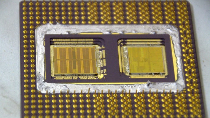
The idea of using a local cache for memory accesses actually originated in the 1960s before the invention of the microprocessor, but they didn't find their way to home computers until the 1980s. It depends on exactly how you define "cache", but while Intel's 80286, Motorola's 68020, and Intel's 80486 processor all have reasonable claims to the title of "first PC CPU with an integrated cache," most people will mark down the 486 as the first consumer chip to have something like the modern conception of a CPU cache. It included 8KB (later 16KB) of on-chip cache, now referred to as L1 cache. Not long after, the Pentium Pro (pictured top), came with both on-die L1 cache and a second silicon die on-package for up to a full megabyte of L2 cache.
These days, processors usually have two or three different "levels" of cache, located in physically distinct locations on the processor die or CPU package. There will typically be an L1 cache located directly inside each CPU core; this is frequently split into separate sections for CPU instructions and data to be processed. The L1 cache is extremely quick to access, and when necessary data or instructions are already cached there, the processor can resume work almost instantly. The downside is that, due to its location it's very small: usually 96KB or less.
Then, there will be an L2 cache either along the edge or outside of the core's functional units, which is shared by both instructions and data. On some processor designs, the L2 cache will be shared across multiple cores, too, like with Intel's current "E-cores" that have a two-to-four megabyte L2 cache shared by each four-core cluster. L2 cache is a bit slower to access than the L1 cache, but the trade off is that it is much, much larger—on the order of an entire megabyte on Zen 4 and a full two megabytes on Raptor Cove.

Next, most processors these days also have an L3 cache that will usually be outside of the core cluster itself. This L3 cache is typically shared by all of the local CPU cores, although many processors today have a split L3 with a portion of the cache attached to each core cluster. You'll see this in AMD's Ryzen processors most notably, where each "Core Complex Die" (CCD) has its own 32MB of L3 cache. Cores on disparate CCDs can access the cache of another CCD, and this is still faster than accessing main memory, but it's quite a bit slower than using the local cache.
Finally, some processors in the past have come with a L4 cache. This is pretty rare, and has only been found on a few processors; primarily, some of IBM POWER family designs and a few Intel chips in the 4th and 5th generations. When present, the L4 cache usually functions like a system-level cache, able to not only cache data for the CPU cores but also possibly for the GPU and other system functions. Some early leaks implied that Intel's Meteor Lake may have had an L4 cache, but the Core Ultra processors to date haven't featured it yet.
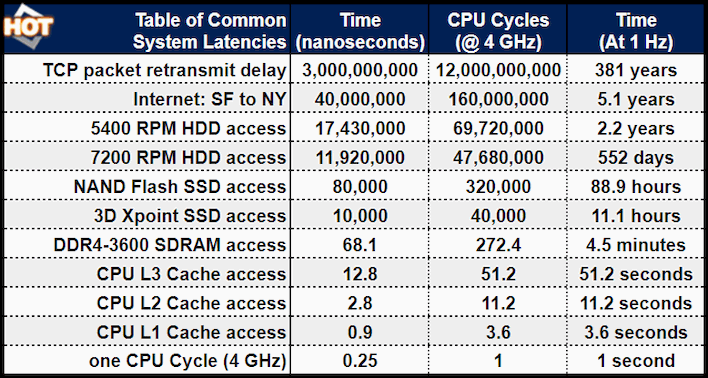
So, modern RAM is super fast, right? With DDR5 we're seeing per-pin speeds as high as 7.5 Gbps. What's the point of CPU cache in the modern age? Well, first of all, CPU cache is way, way faster than that. But moreover, the problem is that, even if you have ultra-low-latency main memory, you're still talking about access times more than five times slower than a CPU's L3 cache—and the L3 itself is nearly five times slower than the L2. Check out the table above for some interesting comparisons.
Most CPU instructions don't complete in a single cycle, but even an access to L1 cache will take around four cycles to complete. If your data isn't present in cache, you'll have to go all the way out to main memory, which will burn up over 270 CPU cycles sitting around waiting. If your data isn't in RAM, it's gonna be a while—might as well switch to another task on that core while you wait, if something else has its data ready to go already. This concept is the basis of multi-tasking, by the way.
If you struggle to comprehend the scope of the big numbers at the top of the chart, check out the last column. This represents the amount of time each operation would take if the same processor were running at one cycle per second instead of four billion cycles per second. This changes the time required for an L2 cache access to 11.2 seconds, which probably still sounds pretty fast compared to the nearly 90 hours required to access an SSD.
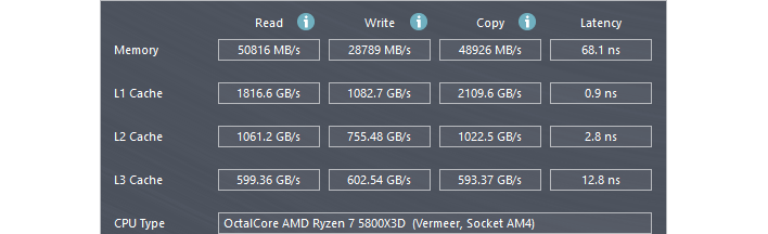
There's more than just latency to consider, though. The above is cropped from an AIDA64 Cache and Memory Benchmark result on the author's PC. As you can see, the transfer rate when reading from the system's 3600 MT/s DDR4 memory is nearly 51 gigabytes per second. Contrast that against the nearly 600 gigabytes per second when reading from L3 cache, and you can start to see how having a large cache can make a huge difference in performance.
This was most visibly demonstrated in recent years by AMD's "X3D" processors sporting 3D V-Cache. By vertically stacking an extra piece of silicon on its Zen 3 "Vermeer" and Zen 4 "Raphael" processors, AMD was able to triple the L3 cache available to one core chiplet, or CCD. Doing this requires modest cuts to CPU clock rate compared to the standard model, yet still yields massive improvements in the performance of certain applications, particularly 3D games. Why is that?

What it comes down to is that, perhaps ironically, video games are some of the most demanding workloads that you can run on a computer. Games are constantly loading in new program fragments and new bits of data to be processed by those program fragments. Because of the immense variety of things happening in a modern 3D game, especially a networked 3D game, it's very easy to overflow the CPU's cache, forcing the app to go out and hit main memory much more often. Tripling the size of Ryzen's already-large L3 cache makes that much less likely, allowing the processor to spend more time working and less time waiting on data or code.
To be clear, there's much more to learn about processor caching. This article is just a basic explainer on the concept of cache and we're not going to go into the weeds explaining the different ways in which caches can be implemented, nor about the different types of processor cache. Ultimately as a consumer what you need to know is that cache size can make an immense difference in application performance, and unlike CPU core count, more is pretty much always better—but if more is pretty much always better, why not just make every processor with huge gobs of cache? Why not just put the whole RAM on the CPU? Well...

Zen 3 CPU core annotation by Locuza. (It's hard to read, so click it to enlarge.)
This annotated die shot of a single Zen 3 CPU core serves to show just how much of a modern processor core is dedicated to cache. Even if we ignore the mostly-blue right half of the core, there are still huge portions of the CPU core carved out for the 32+32K L1 cache and the 512K L2 cache, and then there's that gigantic 4MB of L3 cache, plus all of the associated control hardware.
In short, SRAM (the memory used for cache) is extremely large, and putting a lot of it on the die gobbles up die area very fast. That makes processors get prohibitively expensive to manufacture very quickly. That's why AMD came up with 3D V-Cache: instead of having to make successively larger chips to add progressively larger caches, the company can fabricate separate cache chiplets and staple them onto its existing processors.

We've been focused on AMD for a bit here, but it's not as if Intel is blind to the benefits of processor caches. Intel is the company that's been experimenting on and off with L4 caches, and the biggest change between Golden Cove (the P-core architecture for Alder Lake) and Raptor Cove (the P-core architecture in Raptor Lake) is a 63% increase in the amount of L2 cache available per P-core, with E-cores fully doubling their L2 cache. There aren't many other architectural differences between Intel's 12th- and 13th-Gen Core CPUs, yet Raptor Lake decisively defeats Alder Lake in most applications, especially games. Now, you know why.

Caches are starting to become important in graphics, too. AMD's RDNA 2 family of graphics processors, the Radeon RX 6000 series, used large "Infinity Caches" to make up for their relative lack of memory bandwidth compared to competitor NVIDIA's "Ampere" GPUs. NVIDIA clearly thought this was a good idea, as it radically increased (by a factor of 8) the L2 cache size in its Ada Lovelace architecture to account for slashing memory bus widths on those GPUs in comparison to the previous generation. We can expect to see caching continue to be a critical element in GPU design going forward, and expect NPUs to start developing their own caches soon, too.
Let us know if you found this explainer helpful in any way, if you have any further questions, or if you'd like to correct us about something we slipped up on. Also, if you're interested in seeing more explainer content like this, make sure to drop us a comment saying so.
Photo used in top and thumbnail by Dennis van Zuijlekom, used with permission under CC BY-SA 2.0.