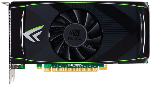
NVIDIA GeForce GTS 450 Affordable DX11 GPU
The most recent NVIDIA GPU released for the desktop market, the GeForce GTX 460, proved to be an excellent performer for the money. In the conclusion of our GTX 460 coverage, we stated, “The GeForce GTX 460 is simply one of the most appealing DirectX 11-class graphics cards out there. They're affordably priced, perform very well, they're a reasonable size and quiet”. Since the GeForce GTX 460 hit the scene a couple of months ago, prices on the cards have dropped somewhat, making them even more attractive. Even with the success of the GTX 460 though, NVIDIA still doesn’t have a sub-$180 DX11 graphics card for the desktop market, and it’s at the more affordable price points that the vast majority of graphics cards are sold.
NVIDIA plans to change that today with the release of the new GeForce GTS 450. As the GTS moniker denotes, the GeForce GTS 450 is targeted at the mainstream market. And with a $129 (give or take) price tag it is certainly more affordable than any other DX11-class GPU. Whether or not it’s worth the asking price remains to be seen, however. So let’s dig in and find out what the new GeForce GTS 450 is made of and if it deserves a place in your next system.
Asus and EVGA Overclocked GeForce GTS 450 Cards
|


The NVIDIA GeForce GTS 450 GPU, Front and Back

Before we show you the actual cards, let’s take a look at the GPU powering the GeForce GTS 450. The chip at the heart of these new cards is codenamed the GF106. It is a new GPU, although it is based on NVIDIA’s Fermi architecture, like the other members of the GeForce GTX/GTS/GT 400 series. The chip is comprised of 1.17 billion transistors and it is manufactured using TSMC’s 40nm process.
Within the chip, as it is configured on the GeForce GTS 450, there is a single Graphics Processing Cluster, with 4 Streaming Multiprocessor segments consisting of 48 CUDA cores. There are 192 CUDA cores in total. There are also 32 texture units and 16 ROPs. GeForce GTS 450 cards also feature a 128-bit memory interface. We should point out, however, that the GF106, as it is implemented on the GeForce GTS 450, isn’t fully functional.
The GF106 diagram above depicts the full GF106 chip architecture that includes one GPC, four SMs, three ROP partitions, and three 64-bit memory interfaces. The GTS 450 GPU is a version of the GF106 chip, but with only two ROP partitions and two memory interface partitions enabled.
NVIDIA goes on to explain, “Our goal with the retail version of GTS 450 is to design the best price/performance product at an aggressive MSRP while offering the highly valued 1GB memory size. The 128-bit memory configuration provides the best price/performance for these design goals.”
Now let's look at the hardware side of things.


